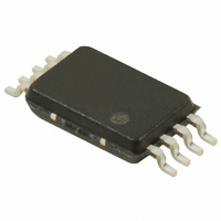
S-35390A-T8T1G Seiko Instruments, S-35390A-T8T1G Datasheet - Page 7

S-35390A-T8T1G
Manufacturer Part Number
S-35390A-T8T1G
Description
IC RTC I2C 2-WIRE 8-TSSOP
Manufacturer
Seiko Instruments
Type
Clock/Calendarr
Datasheet
1.S-35390A-J8T1G.pdf
(56 pages)
Specifications of S-35390A-T8T1G
Time Format
HH:MM:SS (12/24 hr)
Date Format
YY-MM-DD-dd
Interface
I²C, 2-Wire Serial
Voltage - Supply
1.3 V ~ 5.5 V
Operating Temperature
-40°C ~ 85°C
Mounting Type
Surface Mount
Package / Case
8-TSSOP
Function
Clock/Calendar/Alarm/Battery Backup/Interrupt
Supply Voltage (max)
5.5 V
Supply Voltage (min)
1.3 V
Maximum Operating Temperature
+ 85 C
Minimum Operating Temperature
- 40 C
Mounting Style
SMD/SMT
Rtc Bus Interface
Serial (2-Wire, I2C)
Lead Free Status / RoHS Status
Lead free / RoHS Compliant
Memory Size
-
Lead Free Status / Rohs Status
Lead free / RoHS Compliant
Other names
728-1007-2
Available stocks
Company
Part Number
Manufacturer
Quantity
Price
Company:
Part Number:
S-35390A-T8T1G
Manufacturer:
SEIKO
Quantity:
18 700
Part Number:
S-35390A-T8T1G
Manufacturer:
SEIKO
Quantity:
20 000
(Output from S-35390A)
Rev.3.0
(Input from S-35390A)
AC Electrical Characteristics
SCL clock frequency
SCL clock low time
SCL clock high time
SDA output delay time
Start condition setup time
Start condition hold time
Data input setup time
Data input hold time
Stop condition setup time
SCL, SDA rise time
SCL, SDA fall time
Bus release time
Noise suppression time
*1. Since the output format of the SDA pin is Nch open-drain output, SDA output delay time is determined by the values of
*2. Regarding the power supply voltage, refer to “ Recommended Operation Conditions”.
Input pulse voltage
Input pulse rise/fall time
Output determination voltage
Output load
the load resistance (R
SDA
SDA
SCL
_00
Table 7 Measurement Conditions
Parameter
*1
L
) and load capacity (C
t
SU.STA
V
20 ns
V
100 pF + pull-up resistor 1 kΩ
IH
OH
= 0.9 × V
= 0.5 × V
Table 8 AC Electrical Characteristics
t
HD.STA
t
F
DD
Seiko Instruments Inc.
DD
Figure 9 Bus Timing
t
PD
, V
L
, V
f
t
t
t
t
t
t
t
t
t
t
t
t
) outside the IC. Therefore, use this value only as a reference value.
Symbol
SCL
LOW
HIGH
PD
SU.STA
HD.STA
SU.DAT
HD.DAT
SU.STO
R
F
BUF
I
IL
OL
= 0.1 × V
= 0.5 × V
t
HIGH
DD
Min.
250
4.7
4.7
4.7
4.7
DD
0
4
−
4
0
−
−
−
t
V
HD.DAT
DD
*2
t
Typ.
LOW
≥ 1.3 V
−
−
−
−
−
−
−
−
−
−
−
−
−
t
SU.DAT
Remark
SDA
Figure 8 Output Load Circuit
Max.
2-WIRE REAL-TIME CLOCK
100
100
3.5
0.3
−
−
−
−
−
−
−
1
−
The power supplies of the IC
and load have the same
electrical potential.
Min.
100
1.3
0.6
0.6
0.6
0.6
1.3
0
−
0
−
−
−
V
DD
V
*2
DD
Typ.
≥ 3.0 V
−
−
−
−
−
−
−
−
−
−
−
−
−
(Ta = −40 to +85°C)
R = 1 kΩ
C = 100 pF
t
R
t
SU.STO
S-35390A
Max.
400
0.9
0.3
0.3
50
−
−
−
−
−
−
−
−
t
BUF
Unit
kHz
μs
μs
μs
μs
μs
ns
μs
μs
μs
μs
μs
ns
7


