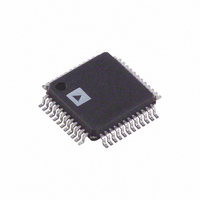
AD9975BST Analog Devices Inc, AD9975BST Datasheet - Page 2

AD9975BST
Manufacturer Part Number
AD9975BST
Description
IC FRONT-END MIXED-SGNL 48-LQFP
Manufacturer
Analog Devices Inc
Series
TxDAC+®r
Datasheet
1.AD9975BST.pdf
(20 pages)
Specifications of AD9975BST
Rohs Status
RoHS non-compliant
Number Of Bits
10
Number Of Channels
1
Voltage - Supply, Analog
3.3V
Voltage - Supply, Digital
3.3V
Package / Case
48-LQFP
Power (watts)
-
Available stocks
Company
Part Number
Manufacturer
Quantity
Price
Company:
Part Number:
AD9975BST
Manufacturer:
ADI
Quantity:
364
AD9975–SPECIFICATIONS
Parameter
OSC IN CHARACTERISTICS
CLOCK OUTPUT CHARACTERISTICS
TX CHARACTERISTICS
RX PATH CHARACTERISTICS (LFP Bypassed)
RX PATH GAIN/OFFSET
RX PATH INPUT CHARACTERISTICS
Frequency Range
Duty Cycle
Input Capacitance
Input Impedance
CLKA Jitter (F
CLKA Duty Cycle
Resolution
Conversion Rate
Pipeline Delay, ADC Clock Cycles
Dynamic Performance (A
Minimum Programmable Gain
Maximum Programmable Gain
Gain Step Size
Gain Step Accuracy
Gain Range Error
Absolute Gain Error, PGA Gain = 0 dB
Input Voltage Range (Gain = –6 dB)
Input Capacitance
Differential Input Resistance
Input Bandwidth (–3 dB) (Rx LPF Bypassed)
Input Referred Noise (at +36 dB Gain with Filter)
Input Referred Noise (at –6 dB Gain with Filter)
Common-Mode Rejection
2× Interpolation Filter Characteristics
TxDAC
@ F
Signal-to-Noise and Distortion Ratio (SINAD)
Effective Number of Bits (ENOB)
Signal-to-Noise Ratio (SNR)
Total Harmonic Distortion (THD)
Spurious-Free Dynamic Range (SFDR)
Narrow Band Rx LPF or Rx LPF Bypassed
Wideband Rx LPF
TX Path Latency, 2× Interpolation
Pass-Band Flatness 0 MHz to 20.7 MHz
Stop-Band Rejection @ 29.3 MHz
Resolution
Conversion Rate
Full-Scale Output Current
Voltage Compliance Range (TX+ or TX– AVSS) Full
Gain Error
Output Offset
Differential Nonlinearity
Integral Nonlinearity
Output Capacitance
Phase Noise @ 1 kHz Offset, 10 MHz Signal
Signal-to-Noise and Distortion (SINAD)
Wideband SFDR (to Nyquist, 50 MHz max)
Narrowband SFDR (3 MHz Window)
5 MHz Analog Out (20 MHz BW)
5 MHz Analog Out
5 MHz Analog Out
IMD (f1 = 6.25 MHz, f2 = 7.8125 MHz)
OSCIN
= 50 MHz, RX LPF Bypassed
CLKA
Derived from PLL)
IN
= –0.5 dBFS, f = 5 MHz)
(V
R
Temp
Full
25°C
25°C
25°C
25°C
25°C
Full
Full
Full
Full
Full
Full
25°C
25°C
25°C
25°C
25°C
25°C
25°C
25°C
25°C
25°C
25°C
N/A
Full
N/A
Full
Full
Full
Full
Full
25°C
25°C
25°C
25°C
25°C
Full
Full
Full
25°C
25°C
25°C
25ºC
25ºC
25ºC
SET
S
= 3.3 V
= 4.02 k , 100
Test
Level
I
II
III
III
II
III
II
II
II
II
II
II
II
II
II
III
II
III
III
II
III
III
III
III
N/A
II
N/A
III
III
III
III
III
I
I
I
I
II
II
II
III
III
III
III
III
III
III
–2–
10%, F
OSCIN
DAC Load.)
Min
10
40
10
2
–0.5
–5.5
0
10
= 50 MHz, F
DAC
50
3
100
14
50 ± 5
10
± 2
2
0.5
5
–100
–60.6
–76.2
–77.9
–77
10
–6
+36
+30
2
± 0.4
± 1.0
± 0.8
4
270
50
Typ
30
0.8
35
10
5.5
–56.6
9.1
–59.2
–60.1
–66
4
16
684
40
= 100 MHz, Gain = –6 dB,
Max
50
60
100
20
+1.5
+5.0
TBD
1
50
Unit
MHz
%
pF
MΩ
ps rms
%
F
dB
dB
Bits
MHz
mA
V
%FS
µA
LSB
LSB
pF
dBc/Hz
dB
dBc
dBc
dBFS
Bits
MHz
Cycles
dB
Bits
dB
dB
dB
dB
dB
dB
dB
dB
dB
dB
Vppd
pF
Ω
MHz
µV rms
µV rms
dB
DAC
Cycles
REV. 0


