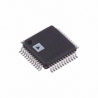
AD9975BST Analog Devices Inc, AD9975BST Datasheet - Page 4

AD9975BST
Manufacturer Part Number
AD9975BST
Description
IC FRONT-END MIXED-SGNL 48-LQFP
Manufacturer
Analog Devices Inc
Series
TxDAC+®r
Datasheet
1.AD9975BST.pdf
(20 pages)
Specifications of AD9975BST
Rohs Status
RoHS non-compliant
Number Of Bits
10
Number Of Channels
1
Voltage - Supply, Analog
3.3V
Voltage - Supply, Digital
3.3V
Package / Case
48-LQFP
Power (watts)
-
Available stocks
Company
Part Number
Manufacturer
Quantity
Price
Company:
Part Number:
AD9975BST
Manufacturer:
ADI
Quantity:
364
AD9975
SPECIFICATIONS
Parameter
SERIAL CONTROL BUS
CMOS LOGIC INPUTS
CMOS LOGIC OUTPUTS (1 mA Load)
POWER SUPPLY
Specifications subject to change without notice.
ABSOLUTE MAXIMUM RATINGS*
Power Supply (V
Digital Output Current . . . . . . . . . . . . . . . . . . . . . . . . . . 5 mA
Digital Inputs . . . . . . . . . . . . . . . . –0.3 V to DRVDD + 0.3 V
Analog Inputs . . . . . . . . . . . . . . . . . –0.3 V to AVDD + 0.3 V
Operating Temperature . . . . . . . . . . . . . . . . . . –40°C to +85°C
Maximum Junction Temperature . . . . . . . . . . . . . . . . . 150°C
Storage Temperature . . . . . . . . . . . . . . . . . . –65°C to +150°C
Lead Temperature (Soldering 10 sec) . . . . . . . . . . . . . . 300°C
*Absolute Maximum Ratings are limiting values to be applied individually and
beyond which the serviceability of the circuit may be impaired. Functional
operability under any of these conditions is not necessarily implied. Exposure to
absolute maximum rating conditions for extended periods of time may affect
device reliability.
Maximum SCLK Frequency (f
Clock Pulsewidth High (t
Clock Pulsewidth Low (t
Clock Rise/Fall Time
Data/Chip-Select Setup Time (t
Data Hold Time (t
Data Valid Time (t
Logic “1” Voltage
Logic “0” Voltage
Logic “1” Current
Logic “0” Current
Input Capacitance
Logic “1” Voltage
Logic “0” Voltage
Digital Output Rise/Fall Time
All Blocks Powered Up
Power Consumption of Functional Blocks
All Blocks Powered Down
I
Digital Supply Current (I
Clock Supply Current (I
Analog Supply Current (I
Rx LPF
ADC and SPGA
Rx Reference
Interpolator
DAC
PLL-A
I
Digital Supply Current (I
Clock Supply Current (I
Analog Supply Current (I
S_TOTAL
S_TOTAL
(Total Supply Current)
(Total Supply Current)
S
) . . . . . . . . . . . . . . . . . . . . . . . . . . . . . . 3.9 V
DH
DV
)
)
(continued)
PWL
PWH
CLKVDD
CLKVDD
DRVDD
DRVDD
AVDD
AVDD
)
)
SCLK
DS
)
)
)
)
+ I
+ I
)
)
DVDD
DVDD
)
)
Temp
Full
Full
Full
Full
Full
Full
Full
25°C
25°C
25°C
25°C
25°C
Full
25°C
Full
25°C
25°C
25°C
25°C
25°C
25°C
25°C
25°C
25°C
25°C
25°C
25°C
25°C
25°C
Test
Level
II
II
II
II
II
II
II
II
II
II
II
III
II
II
II
I
III
III
III
III
III
III
III
III
III
I
III
III
III
–4–
EXPLANATION OF TEST LEVELS
I. Devices are 100% production tested at 25°C and guaranteed
II. Parameter is guaranteed by design and/or characterization
III. Parameter is a typical value only.
THERMAL CHARACTERISTICS
Thermal Resistance
48-Lead LQFP
θ
θ
JA
JC
by design and characterization testing for the commercial
operating temperature range (–40°C to +85°C).
testing.
= 57ºC/W
= 28ºC/W
Min
25
18
18
25
0
V
V
1.5
DRVDD
DRVDD
– 0.7
– 0.6
3
210
22.5
5.5
182
110
55
2
20
18
22
21
10
0
11
Typ
Max
10
20
0.4
12
12
0.4
2.5
227
27
Unit
MHz
ns
ns
µs
ns
ns
ns
V
V
µA
µA
pF
V
V
ns
mA
mA
mA
mA
mA
mA
mA
mA
mA
mA
mA
mA
mA
REV. 0


