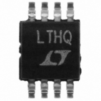
LTC1864CMS8#PBF Linear Technology, LTC1864CMS8#PBF Datasheet

LTC1864CMS8#PBF
Specifications of LTC1864CMS8#PBF
Related parts for LTC1864CMS8#PBF
LTC1864CMS8#PBF Summary of contents
Page 1
... Portable or Compact Instrumentation n Low Power Battery-Operated Instrumentation n Isolated and/or Remote Data Acquisition L, LT, LTC and LTM are registered trademarks of Linear Technology Corporation. All other trademarks are the property of their respective owners. TYPICAL APPLICATION Single 5V Supply, 250ksps, 16-Bit Sampling ADC 1μF 5V LTC1864 ...
Page 2
... REF + 2 IN – GND S8 PACKAGE 8-LEAD PLASTIC 150°C, θ = 175°C/W JMAX JA ORDER INFORMATION LEAD FREE FINISH TAPE AND REEL LTC1864CMS8#PBF LTC1864CMS8#TRPBF LTC1864IMS8#PBF LTC1864IMS8#TRPBF LTC1864HMS8#PBF LTC1864HMS8#TRPBF LTC1864ACMS8#PBF LTC1864ACMS8#TRPBF LTC1864AIMS8#PBF LTC1864AIMS8#TRPBF LTC1864AHMS8#PBF LTC1864AHMS8#TRPBF LTC1864CS8#PBF LTC1864CS8#TRPBF LTC1864IS8#PBF LTC1864IS8#TRPBF LTC1864ACS8#PBF LTC1864ACS8#TRPBF LTC1684AIS8#PBF LTC1684AIS8#TRPBF ...
Page 3
ORDER INFORMATION LEAD FREE FINISH TAPE AND REEL LTC1865HMS#PBF LTC1865HMS#TRPBF LTC1865ACMS#PBF LTC1865ACMS#TRPBF LTC1865AIMS#PBF LTC1865AIMS#TRPBF LTC1865AHMS#PBF LTC1865AHMS#TRPBF LTC1865CS8#PBF LTC1865CS8#TRPBF LTC1865IS8#PBF LTC1865IS8#TRPBF LTC1865ACS8#PBF LTC1865ACS8#TRPBF LTC1865AIS8#PBF LTC1865AIS8#TRPBF LEAD BASED FINISH TAPE AND REEL LTC1864CMS8 LTC1864CMS8#TR LTC1864IMS8 LTC1864IMS8#TR LTC1864HMS8 LTC1864HMS8#TR LTC1864ACMS8 LTC1864ACMS8#TR LTC1864AIMS8 LTC1864AIMS8#TR ...
Page 4
LTC1864/LTC1865 CONVERTER AND MULTIPILEXER CHARACTERISTICS l The denotes the specifi cations which apply over the full operating temperature range, otherwise specifi cations are 5V 5V defi ned in Recommended Operating ...
Page 5
DIGITAL AND DC ELECTRICAL CHARACTERISTICS over the full operating temperature range, otherwise specifi cations are T SYMBOL PARAMETER V High Level Input Voltage IH V Low Level Input Voltage IL I High Level Input Current IH I Low Level Input ...
Page 6
LTC1864/LTC1865 RECOMMENDED OPERATING CONDITIONS full operating temperature range, otherwise specifi cations are T SYMBOL PARAMETER V Supply Voltage CC f Clock Frequency SCK t Total Cycle Time CYC t Analog Input Sampling Time SMPL t Setup Time CONV↓ Before First ...
Page 7
TIMING CHARACTERISTICS range, otherwise specifi cations are T = 25° unless otherwise noted. SYMBOL PARAMETER t Conversion Time (See Figure 1) CONV f Maximum Sampling Frequency SMPL(MAX) t Delay Time, SCK↓ to SDO Data Valid dDO t Delay ...
Page 8
LTC1864/LTC1865 TYPICAL PERFORMANCE CHARACTERISTICS Supply Current vs Sampling Frequency 1000 25°C A CONV LOW = 800ns 100 10 1 0.1 0.01 0.01 0.1 1.0 10 100 SAMPLING FREQUENCY (kHz) 18645 G01 Reference Current vs ...
Page 9
TYPICAL PERFORMANCE CHARACTERISTICS Change in Offset Error vs Reference Voltage 25° – REFERENCE VOLTAGE (V) 18645 G10 Change in Gain Error vs Temperature 5 ...
Page 10
LTC1864/LTC1865 PIN FUNCTIONS LTC1864 V (Pin 1): Reference Input. The reference input defi nes REF the span of the A/D converter and must be kept free of noise with respect to GND. + – (Pins 2, 3): ...
Page 11
FUNCTIONAL BLOCK DIAGRAM PIN NAMES IN PARENTHESES REFER TO LTC1865 + IN (CH0) – IN (CH1) GND V CC CONV (SDI) SCK CONVERT BIAS AND CLK SHUTDOWN DATA IN + 16-BIT SAMPLING DATA OUT ADC – V REF LTC1864/LTC1865 SDO ...
Page 12
LTC1864/LTC1865 TEST CIRCUITS Load Circuit for dDO r f TEST POINT V 3k SDO t 20pF Voltage Waveforms for t CONV SDO t en Voltage Waveforms for SDO Delay Times,t SCK V IL ...
Page 13
APPLICATIONS INFORMATION LTC1864 OPERATION Operating Sequence The LTC1864 conversion cycle begins with the rising edge of CONV. After a period equal to t CONV fi nished. If CONV is left high after this time, the LTC1864 goes into sleep mode ...
Page 14
LTC1864/LTC1865 APPLICATIONS INFORMATION LTC1865 OPERATION Operating Sequence The LTC1865 conversion cycle begins with the rising edge of CONV. After a period equal to t CONV fi nished. If CONV is left high after this time, the LTC1865 goes into sleep ...
Page 15
APPLICATIONS INFORMATION GENERAL ANALOG CONSIDERATIONS Grounding The LTC1864/LTC1865 should be used with an analog ground plane and single point grounding techniques. Do not use wire wrapping techniques to breadboard and evaluate the device. To achieve the optimum performance, use a ...
Page 16
LTC1864/LTC1865 APPLICATIONS INFORMATION 16 18645fb ...
Page 17
APPLICATIONS INFORMATION Component Side Silk Screen for LTC1864 Evaluation Circuit Component Side Showing Traces (Note Sider Traces on Analog Side) Ground Layer with Separate Analog and Digital Grounds LTC1864/LTC1865 Bottom Side Showing Traces (Note Almost No Analog Traces on Board ...
Page 18
LTC1864/LTC1865 APPLICATIONS INFORMATION REFERENCE DIG U12A 74AC109 U9B 74AC00 CLK 1 CLR 5 PRE 5V U9A DIG 74AC00 C16 0.1μF 5V DIG 5V DIG U6 U7 ...
Page 19
APPLICATIONS INFORMATION V V IC1A CC CC 74AC74 4 5 PRE Q DATA CLK 10 CLK PRE CLR D CLK 11 CLK CLR IC1B 74AC74 RECEIVE CLOCK ...
Page 20
LTC1864/LTC1865 APPLICATIONS INFORMATION Transmit LTC1864 Data Over Modular Telephone Wire Using Simple Transmitter/Receiver Figure 6 shows a simple Manchester encoder and dif- ferential transmitter suitable for use with the LTC1864. This circuit allows transmission of data over inexpensive telephone wire. ...
Page 21
PACKAGE DESCRIPTION 0.889 ± 0.127 (.035 ± .005) 5.23 3.2 – 3.45 (.206) (.126 – .136) MIN 0.65 0.42 ± 0.04 (.0256) (.0165 ± .0015) TYP BSC RECOMMENDED SOLDER PAD LAYOUT NOTE: 1. DIMENSIONS IN MILLIMETER/(INCH) 2. DRAWING NOT TO ...
Page 22
LTC1864/LTC1865 PACKAGE DESCRIPTION 0.889 ± 0.127 (.035 ± .005) 5.23 3.2 – 3.45 (.206) (.126 – .136) MIN 0.305 ± 0.038 0.50 (.0120 ± .0015) (.0197) TYP BSC RECOMMENDED SOLDER PAD LAYOUT NOTE: 1. DIMENSIONS IN MILLIMETER/(INCH) 2. DRAWING NOT ...
Page 23
... FLASH SHALL NOT EXCEED 0.010" (0.254mm) PER SIDE Information furnished by Linear Technology Corporation is believed to be accurate and reliable. However, no responsibility is assumed for its use. Linear Technology Corporation makes no representa- tion that the interconnection of its circuits as described herein will not infringe on existing patent rights. ...
Page 24
... Slew Rate, 3.5nV/√Hz Noise, –80dBc Distortion 350V/μs Slew Rate, –90dBc Distortion at 5MHz www.linear.com ● 4096 Point FFT of Output 7.507324kHz AT 530mV 1 P 45.007324kHz AT 1. 100kHz 100 110 120 130 FREQUENCY (kHz) 18645 TA03b 18645fb LT 1207 REV B • PRINTED IN USA © LINEAR TECHNOLOGY CORPORATION 2007 ...


