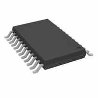
AD7190BRUZ Analog Devices Inc, AD7190BRUZ Datasheet - Page 35

AD7190BRUZ
Manufacturer Part Number
AD7190BRUZ
Description
IC ADC 2CH 24BIT W/PGA 24TSSOP
Manufacturer
Analog Devices Inc
Datasheet
1.AD7190BRUZ.pdf
(40 pages)
Specifications of AD7190BRUZ
Data Interface
DSP, MICROWIRE™, QSPI™, Serial, SPI™
Design Resources
Precision Weigh Scale Design Using AD7190 with Internal PGA (CN0102)
Number Of Bits
24
Sampling Rate (per Second)
4.8k
Number Of Converters
1
Voltage Supply Source
Analog and Digital
Operating Temperature
-40°C ~ 105°C
Mounting Type
Surface Mount
Package / Case
24-TSSOP (0.173", 4.40mm Width)
Resolution (bits)
24bit
Sampling Rate
4.8kSPS
Input Channel Type
Pseudo Differential
Supply Voltage Range - Analog
4.75V To 5.25V
Lead Free Status / RoHS Status
Lead free / RoHS Compliant
Available stocks
Company
Part Number
Manufacturer
Quantity
Price
Company:
Part Number:
AD7190BRUZ
Manufacturer:
ADI
Quantity:
1 000
Part Number:
AD7190BRUZ
Manufacturer:
ADI/亚德诺
Quantity:
20 000
Company:
Part Number:
AD7190BRUZ-REEL
Manufacturer:
ADI
Quantity:
1 000
Part Number:
AD7190BRUZ-REEL
Manufacturer:
ADI/亚德诺
Quantity:
20 000
SYSTEM SYNCHRONIZATION
The SYNC input allows the user to reset the modulator and the
digital filter without affecting any of the setup conditions on the
part. This allows the user to start gathering samples of the analog
input from a known point in time, that is, the rising edge of
SYNC . SYNC needs to be taken low for four master clock cycles
to implement the synchronization function.
If multiple AD7190 devices are operated from a common master
clock, they can be synchronized so that their data registers are
updated simultaneously. A falling edge on the SYNC pin resets
the digital filter and the analog modulator and places the AD7190
into a consistent, known state. While the SYNC pin is low, the
AD7190 is maintained in this state. On the SYNC rising edge,
the modulator and filter are taken out of this reset state and, on
the next clock edge, the part starts to gather input samples again.
In a system using multiple AD7190 devices, a common signal to
their SYNC pins synchronizes their operation. This is normally
done after each AD7190 has performed its own calibration or
has had calibration coefficients loaded into its calibration
registers. The conversions from the AD7190s are then
synchronized.
The part is taken out of reset on the master clock falling edge
following the SYNC low-to-high transition. Therefore, when
multiple devices are being synchronized, the SYNC pin should
be taken high on the master clock rising edge to ensure that all
devices begin sampling on the master clock falling edge. If the
SYNC pin is not taken high in sufficient time, it is possible to
have a difference of one master clock cycle between the devices;
that is, the instant at which conversions are available differs
from part to part by a maximum of one master clock cycle.
The SYNC pin can also be used as a start conversion command.
In this mode, the rising edge of SYNC starts conversion, and the
falling edge of RDY indicates when the conversion is complete.
The disadvantage of this scheme is that the settling time of the
filter has to be allowed for each data register update. This means
that the rate at which the data register is updated is reduced. For
example, if the ADC is configured to use the sinc
latency is disabled and chop is disabled, the data register update
takes four times longer.
4
filter, zero
Rev. B | Page 35 of 40
TEMPERATURE SENSOR
Embedded in the AD7190 is a temperature sensor. This is
selected using the CH2 bit in the configuration register. When
the CH2 bit is set to 1, the temperature sensor is enabled. When
the temperature sensor is selected and bipolar mode is selected,
the device should return a code of 0x800000 when the temper-
ature is 0 K. A one-point calibration is needed to get the optimum
performance from the sensor. Therefore, a conversion at 25°C
should be recorded and the sensitivity calculated. The sensitivity
is approximately 2815 codes/°C. The equation for the temperature
sensor is
Following the one point calibration, the internal temperature
sensor has an accuracy of ±2 °C, typically.
BRIDGE POWER-DOWN SWITCH
In bridge applications such as strain gauges and load cells, the
bridge itself consumes the majority of the current in the system.
For example, a 350 Ω load cell requires 15 mA of current when
excited with a 5 V supply. To minimize the current consumption
of the system, the bridge can be disconnected (when it is not
being used) using the bridge power-down switch. Figure 18
shows how the bridge power-down switch is used. The switch
can withstand 30 mA of continuous current, and it has an on
resistance of 10 Ω maximum.
LOGIC OUTPUTS
The AD7190 has four general-purpose digital outputs, P0, P1,
P2, and P3. These are enabled using the GP32EN and GP10EN
bits in the GPOCON register. The pins can be pulled high or
low using the P0DAT to P3DAT bits in the GPOCON register;
that is, the value at the pin is determined by the setting of the
P0DAT to P3DAT bits. The logic levels for these pins are
determined by AV
register is read, the P0DAT to P3DAT bits reflect the actual
value at the pins. This is useful for short-circuit detection.
These pins can be used to drive external circuitry, for example,
an external multiplexer. If an external multiplexer is used to
increase the channel count, the multiplexer logic pins can be
controlled via the AD7190 general-purpose output pins. The
general-purpose output pins can be used to select the active
multiplexer pin. Because the operation of the multiplexer is
independent of the AD7190, the AD7190 modulator and filter
should be reset using the SYNC pin each time that the multi-
plexer channel is changed.
Temp (K) = (Conversion – 0x800000)/2815 K
Temp (°C) = Temp (K) – 273
DD
rather than by DV
DD
. When the GPOCON
AD7190


