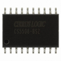
CS5508-BSZ Cirrus Logic Inc, CS5508-BSZ Datasheet - Page 13

CS5508-BSZ
Manufacturer Part Number
CS5508-BSZ
Description
IC ADC 20BIT LOW PWR 20-SOIC
Manufacturer
Cirrus Logic Inc
Datasheet
1.CS5507-ASZ.pdf
(40 pages)
Specifications of CS5508-BSZ
Data Interface
Serial
Number Of Bits
20
Sampling Rate (per Second)
100
Number Of Converters
1
Power Dissipation (max)
4.5mW
Voltage Supply Source
Analog and Digital, Dual ±
Operating Temperature
-40°C ~ 85°C
Mounting Type
Surface Mount
Package / Case
20-SOIC
Resolution (bits)
20bit
Sampling Rate
100SPS
Input Channel Type
Differential
Supply Current
340µA
Digital Ic Case Style
SOIC
No. Of Pins
20
Lead Free Status / RoHS Status
Lead free / RoHS Compliant
Other names
598-1099-5
Available stocks
Company
Part Number
Manufacturer
Quantity
Price
Part Number:
CS5508-BSZ
Manufacturer:
CIRRUS
Quantity:
20 000
GENERAL DESCRIPTION
The CS5505/6/7/8 are very low power mono-
lith ic CM OS A/D co nverters designed
specifically for measurement of dc signals. The
CS5505/7 are 16-bit converters (a four channel
and a single channel version). The CS5506/8 are
20-bit converters (a four channel and a single
channel version). Each of the devices includes a
delta-sigma charge-balance converter, a voltage
reference, a calibration microcontroller with
SRAM, a digital filter and a serial interface. The
CS5505 and CS5506 include a four channel
pseudo-differential (all four channels have the
same reference measurement node) multiplexer.
The CS5505/6/7/8 include an on-chip reference
but can also utilize an off-chip reference for pre-
cision applications. The CS5505/6/7/8 can be
used to measure either unipolar or bipolar sig-
nals. The devices use self-calibration to insure
excellent offset and gain accuracy.
The CS5505/6/7/8 are optimized to operate from
a 32.768 kHz crystal but can be driven by an
external clock whose frequency is between
30 kHz and 163 kHz. When the digital filter is
operated with a 32.768 kHz clock, the filter has
zeros precisely at 50 and 60 Hz line frequencies
and multiples thereof.
The CS5505/6/7/8 use a "start convert" com-
mand to latch the input channel selection and to
start a convolution cycle on the digital filter.
Once the filter cycle is completed, the output
port is updated. When operated with a
32.768 kHz clock the ADC converts and updates
its output port at 20 samples/sec. The throughput
rate per channel is the output update rate divided
by th e number of channels being multi-
plexed. The output port includes a serial
interface with two modes of operation.
The CS5505/6/7/8 can operate from dual polar-
ity power supplies (+5 and -5), from a single +5
volt supply, or with +10 volts on the analog and
DS59F7
DS59F4
+5 on the digital. They can also operate with
dual polarity (+5 and -5), or from a single +5
volt supply on the analog and + 3.3 on the digi-
tal.
THEORY OF OPERATION FOR THE
CS5505/6/7/8
The front page of this data sheet illustrates the
block diagram of the CS5505/6.
Basic Converter Operation
The CS5505/6/7/8 A/D converters have four op-
erating states. These are start-up, calibration,
conversion and sleep. When power is first ap-
plied, the device enters the start-up state. The
first step is a power-on reset delay of about
10 ms which resets all of the logic in the device.
To proceed with start-up, the oscillator must
then begin oscillating. After the power-on reset
the device enters the wake-up period for 1800
clock cycles after clock is present. This allows
the delta-sigma modulator and other circuitry
(which are operating with very low currents) to
reach a stable bias condition prior to entering
into either the calibration or conversion states.
During the 1800 cycle wake-up period, the de-
vice can accept an input command. Execution of
this command will not occur until the complete
wake-up period elapses. If no command is given,
the device enters the standby mode.
Calibration
After the initial application of power, the
CS5505/6/7/8 must enter the calibration state
prior to performing accurate conversions. During
calibration, the chip executes a two-step process.
The device first performs an offset calibration
and then follows this with a gain calibration.
The two calibration steps determine the zero ref-
erence point and the full scale reference point of
the converter’s transfer function. From these
points it calibrates the zero point and a gain
CS5505/6/7/8
CS5505/6/7/8
13
13


