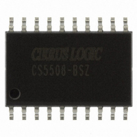
CS5508-BSZ Cirrus Logic Inc, CS5508-BSZ Datasheet - Page 21

CS5508-BSZ
Manufacturer Part Number
CS5508-BSZ
Description
IC ADC 20BIT LOW PWR 20-SOIC
Manufacturer
Cirrus Logic Inc
Datasheet
1.CS5507-ASZ.pdf
(40 pages)
Specifications of CS5508-BSZ
Data Interface
Serial
Number Of Bits
20
Sampling Rate (per Second)
100
Number Of Converters
1
Power Dissipation (max)
4.5mW
Voltage Supply Source
Analog and Digital, Dual ±
Operating Temperature
-40°C ~ 85°C
Mounting Type
Surface Mount
Package / Case
20-SOIC
Resolution (bits)
20bit
Sampling Rate
100SPS
Input Channel Type
Differential
Supply Current
340µA
Digital Ic Case Style
SOIC
No. Of Pins
20
Lead Free Status / RoHS Status
Lead free / RoHS Compliant
Other names
598-1099-5
Available stocks
Company
Part Number
Manufacturer
Quantity
Price
Part Number:
CS5508-BSZ
Manufacturer:
CIRRUS
Quantity:
20 000
with other crystals in the range of 30 kHz to
53 kHz.
55 to +125 °C) the on-chip gate oscillator is
designed to work only with a 32.768 kHz crys-
tal.
frequencies from 30 kHz to 163
temperature ranges.
normally specified as a time-keeping crystal with
tight specifications for both initial frequency and
for drift over temperature. To maintain excellent
frequency stability, these crystals are specified
only over limited operating temperature ranges
(i.e. -10 to +60 °C) by the manufacturers. Appli-
cations of these crystals with the CS5505/6/7/8
do not require tight initial tolerance or low
tempco drift. Therefore, a lower cost crystal with
looser initial tolerance and tempco will generally
be adequate for use with the CS5505/6/7/8 con-
verters. Also check with the manufacturer about
wide temperature range application of their
standard crystals. Generally, even those crystals
specified for limited temperature range will op-
erate over much larger ranges if frequency
stability over temperature is not a requirement.
The frequency stability can be as bad as ±3000
ppm over the operating temperature range and
still be typically better than the line frequency
(50 or 60 Hz) stability over cycle to cycle during
the course of a day.
for operation over the military temperature range
(-55 to +125 °C). See the Appendix for suppliers
of 32.768 kHz crystals.
Serial Interface Logic
The digital filter in the CS5505/6/7/8 takes 1624
clock cycles to compute an output word once a
conversion begins. At the end of the conversion
cycle, the filter will attempt to update the serial
port. Two clock cycles prior to the update
DRDY will go high. When DRDY goes high
just prior to a port update it checks to see if the
port is either empty or unselected (CS = 1). If
the port is empty or unselected, the digital filter
will update the port with a new output word.
DS59F7
DS59F4
The chip will operate with external clock
Over the military temperature range (-
The 32.768 kHz crystal is
There are crystals available
kHz.over all
When new data is put into the port DRDY will
go low.
Data can be read from the serial port in either of
two modes. The M/SLP pin determines which
serial mode is selected. Serial port mode selec-
tion is as follows:
SSC (Synchronous Self-Clocking) mode;
M/SLP = VD+, or SEC (Synchronous External
Clocking) mode; M/SLP = DGND. Timing dia-
grams which illustrate the SSC and SEC timing
are in the tables section of this data sheet.
Synchronous Self-Clocking Mode
The serial port operates in the SSC mode when
the M/SLP pin is connected to the VD+ pin on
the part. In SSC mode the CS5505/6/7/8 fur-
nishes both the serial output data (SDATA) and
the serial clock (SCLK). When the serial port is
updated at the end of a conversion, DRDY falls.
If CS is low, the SDATA and SCLK pins will
come out of the high impedance state two XIN
clock cycles after DRDY falls. The MSB data
bit will be presented for two cycles of XIN
clock. The SCLK signal will rise in the middle
of the MSB data bit. When SCLK then returns
low the (MSB - 1) bit will appear. Subsequent
data bits will be output on each falling edge of
SCLK until the LSB data bit is output. After the
LSB data bit is output, the SCLK will fall at
which time both the SDATA and SCLK outputs
will return to the high impedance output state.
DRDY will return high at this time.
If CS is taken low after DRDY falls, the MSB
data bit will appear within two XIN clock cycles
after CS is taken low. CS need not be held low
for the entire data output. If CS is returned high
during a data bit the port will complete the out-
put of that bit and then go into the Hi-Z state.
The port can be reselected any time prior to the
completion of the next conversion (DRDY fall-
ing) to allow the remaining data bits to be
output.
CS5505/6/7/8
CS5505/6/7/8
21
21


