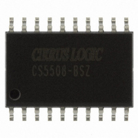
CS5508-BSZ Cirrus Logic Inc, CS5508-BSZ Datasheet - Page 34

CS5508-BSZ
Manufacturer Part Number
CS5508-BSZ
Description
IC ADC 20BIT LOW PWR 20-SOIC
Manufacturer
Cirrus Logic Inc
Datasheet
1.CS5507-ASZ.pdf
(40 pages)
Specifications of CS5508-BSZ
Data Interface
Serial
Number Of Bits
20
Sampling Rate (per Second)
100
Number Of Converters
1
Power Dissipation (max)
4.5mW
Voltage Supply Source
Analog and Digital, Dual ±
Operating Temperature
-40°C ~ 85°C
Mounting Type
Surface Mount
Package / Case
20-SOIC
Resolution (bits)
20bit
Sampling Rate
100SPS
Input Channel Type
Differential
Supply Current
340µA
Digital Ic Case Style
SOIC
No. Of Pins
20
Lead Free Status / RoHS Status
Lead free / RoHS Compliant
Other names
598-1099-5
Available stocks
Company
Part Number
Manufacturer
Quantity
Price
Part Number:
CS5508-BSZ
Manufacturer:
CIRRUS
Quantity:
20 000
34
Introduction
The CDB5505/6/7/8 evaluation board provides a
quick means of testing the CS5505/6/7/8 series
A/D converters. The CS5505/6/7/8 converters
require a minimal amount of external circuitry.
The evaluation board comes configured with the
A/D converter chip operating from a 32.768 kHz
crystal and with an off-chip precision 2.5 volt
reference. The board provides access to all of
the digital interface pins of the CS5505/6/7/8
chip.
The board is configured for operation from +5
and -5 volt power supplies, but can be operated
from a single +5 volt supply if the -5V binding
post is shorted to the GND binding post.
Evaluation Board Overview
The board provides a complete means of making
the CS5505/6/7/8 A/D converter chip function.
The user must provide a means of taking the
output data from the board in serial format and
using it in his system.
Figure 1 illustrates the schematic for the board.
The board comes configured for the A/D con-
verter chip to operate from the 32.768 kHz
watch crystal. A BNC connector for an external
clock is provided on the board. To connect the
external BNC source to the converter chip, a cir-
cuit trace must be cut. Then a jumper must be
inserted in the proper holes to connect the XIN
pin of the converter to the input line from the
BNC. The BNC input is terminated with a 50Ω
resistor. Remove this resistor if driving from a
logic gate. See the schematic in Figure 1.
The board comes with the A/D converter
VREF+ and VREF- pins hard-wired to the
2.5 volt bandgap voltage reference IC on the
board. The VREF+ and VREF- pins can be con-
nected to either the on chip reference or an
34
off-board reference if the connections (2A and
2B) to the bandgap IC are cut.
Note that the pin-out of the CS5505/6/7/8 series
chips allows the 20-pin single channel devices to
be plugged into the 24-pin, four channel foot-
print. See Figure 2 which illustrates the footprint
compatibility.
Prior to powering up the board, select the serial
port operating mode with the appropriate jumper
on the M/SLP header. The device can be oper-
ated in either the SSC (Synchronous
Self-Clocking) or the SEC (Synchronous Exter-
nal Clocking) mode. See the device data sheet
for an explanation of these modes.
All of the control pins of the CS5505/6/7/8 are
available at the J1 header connector. Buffer ICs
U2 and U3 are used to buffer the converter for
interface to off-board circuits. The buffers are
used on the evaluation board only because the
exact loading and off-board circuitry is un-
known. Most applications will not require the
buffer ICs for proper operation.
To put the board in operation, select either bipo-
lar or unipolar mode with DIP switch S2. Then
press the CAL pushbutton after the board is
powered up. This initiates calibration of the con-
verter which is required before measurements
can be taken.
To select an input channel on the four channel
devices, use DIP switch S2 to select the inputs
A1
0
0
1
1
Table 1. Multiplexer Truth Table
A0
0
1
0
1
CDB5505/6/7/8
Channel addressed
AIN1
AIN2
AIN3
AIN4
CS5505/6/7/8
DS59DB4
DS59DB2


