ADC08D500CIYB/NOPB National Semiconductor, ADC08D500CIYB/NOPB Datasheet - Page 14
ADC08D500CIYB/NOPB
Manufacturer Part Number
ADC08D500CIYB/NOPB
Description
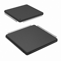
IC ADC 8BIT 500MSPS DUAL 128LQFP
Manufacturer
National Semiconductor
Series
PowerWise®r
Specifications of ADC08D500CIYB/NOPB
Number Of Bits
8
Sampling Rate (per Second)
500M
Data Interface
Serial
Number Of Converters
2
Power Dissipation (max)
1.78W
Voltage Supply Source
Single Supply
Operating Temperature
-40°C ~ 85°C
Mounting Type
Surface Mount
Package / Case
128-LQFP Exposed Pad
Lead Free Status / RoHS Status
Lead free / RoHS Compliant
Other names
*ADC08D500CIYB
*ADC08D500CIYB/NOPB
ADC08D500CIYB
*ADC08D500CIYB/NOPB
ADC08D500CIYB
Available stocks
Company
Part Number
Manufacturer
Quantity
Price
Company:

Part Number:
ADC08D500CIYB/NOPB
Manufacturer:
Texas Instruments
Quantity:
10 000


Note 9: Calculation of Full-Scale Error for this device assumes that the actual reference voltage is exactly its nominal value. Full-Scale Error for this device,
therefore, is a combination of Full-Scale Error and Reference Voltage Error. See Transfer Characteristic
Figure
2. For relationship between Gain Error and Full-
Scale Error, see Specification Definitions for Gain Error.
Note 10: The analog and clock input capacitances are die capacitances only. Additional package capacitances of 0.65 pF differential and 0.95 pF each pin to
ground are isolated from the die capacitances by lead and bond wire inductances.
Note 11: This parameter is guaranteed by design and is not tested in production.
Note 12: This parameter is guaranteed by design and/or characterization and is not tested in production.
Note 13: The digital control pin capacitances are die capacitances only. Additional package capacitance of 1.6 pF each pin to ground are isolated from the die
capacitances by lead and bond wire inductances.
Note 14: Each of the two converters of the ADC08D500 has two LVDS output buses, which each clock data out at one half the sample rate. The data at each
bus is clocked out at one half the sample rate. The second bus (D0 through D7) has a pipeline latency that is one clock cycle less than the latency of the first bus
(Dd0 through Dd7)
Note 15: Tying V
to the supply rail will increase the output offset voltage (V
) by 400mv (typical), as shown in the V
specification above. Tying V
to the
BG
OS
OS
BG
supply rail will also affect the differential LVDS output voltage (V
), causing it to increase by 40mV (typical).
OD
13
www.national.com
Related parts for ADC08D500CIYB/NOPB
Image
Part Number
Description
Manufacturer
Datasheet
Request
R

Part Number:
Description:
National Semiconductor [8-Bit D/A Converter]
Manufacturer:
National Semiconductor
Datasheet:
Part Number:
Description:
National Semiconductor [Media Coprocessor]
Manufacturer:
National Semiconductor
Datasheet:
Part Number:
Description:
Digitally Controlled Tone and Volume Circuit with Stereo Audio Power Amplifier, Microphone Preamp Stage and National 3D Sound
Manufacturer:
National Semiconductor
Datasheet:
Part Number:
Description:
Digitally Controlled Tone and Volume Circuit with Stereo Audio Power Amplifier, Microphone Preamp Stage and National 3D Sound
Manufacturer:
National Semiconductor
Datasheet:
Part Number:
Description:
AC97 Rev 2 Codec with Sample Rate Conversion and National 3D Sound
Manufacturer:
National Semiconductor
Part Number:
Description:
Manufacturer:
National Semiconductor
Datasheet:
Part Number:
Description:
Manufacturer:
National Semiconductor
Datasheet:
Part Number:
Description:
General Purpose, Low Voltage, Low Power, Rail-to-Rail Output Operational Amplifiers
Manufacturer:
National Semiconductor
Datasheet:
Part Number:
Description:
8-bit 20 MSPS flash A/D converter.
Manufacturer:
National Semiconductor
Datasheet:
Part Number:
Description:
Low Noise Quad Operational Amplifier
Manufacturer:
National Semiconductor
Datasheet:
Part Number:
Description:
Quad Differential Line Receivers
Manufacturer:
National Semiconductor
Datasheet:
Part Number:
Description:
Quad High Speed Trapezoidal? Bus Transceiver
Manufacturer:
National Semiconductor
Datasheet:
Part Number:
Description:
Dual Line Receiver
Manufacturer:
National Semiconductor
Datasheet:
Part Number:
Description:
TTL to 10k ECL Level Translator with Latch
Manufacturer:
National Semiconductor
Datasheet: