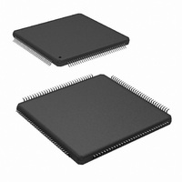
ADC08D500CIYB/NOPB National Semiconductor, ADC08D500CIYB/NOPB Datasheet - Page 28

ADC08D500CIYB/NOPB
Manufacturer Part Number
ADC08D500CIYB/NOPB
Description
IC ADC 8BIT 500MSPS DUAL 128LQFP
Manufacturer
National Semiconductor
Series
PowerWise®r
Specifications of ADC08D500CIYB/NOPB
Number Of Bits
8
Sampling Rate (per Second)
500M
Data Interface
Serial
Number Of Converters
2
Power Dissipation (max)
1.78W
Voltage Supply Source
Single Supply
Operating Temperature
-40°C ~ 85°C
Mounting Type
Surface Mount
Package / Case
128-LQFP Exposed Pad
Lead Free Status / RoHS Status
Lead free / RoHS Compliant
Other names
*ADC08D500CIYB
*ADC08D500CIYB/NOPB
ADC08D500CIYB
*ADC08D500CIYB/NOPB
ADC08D500CIYB
Available stocks
Company
Part Number
Manufacturer
Quantity
Price
Company:
Part Number:
ADC08D500CIYB/NOPB
Manufacturer:
Texas Instruments
Quantity:
10 000
1.4 REGISTER DESCRIPTION
Eight write-only registers provide several control and config-
uration options in the Extended Control Mode. These regis-
ters have no effect when the device is in the Normal Control
Mode. Each register description below also shows the Power-
On Reset (POR) state of each control bit.
IMPORTANT: The Configuration Register should not be
written if the DES Enable bit = 1. The DES Enable bit
should first be changed to 0, then the Configuration
Register can be written. Failure to follow this procedure
can cause the internal DES clock generation circuitry to
stop.
Bit 15
Bit 14
Bit 13
Bit 12
Bit 11
Bit 10
Bit 9
Addr: 1h (0001b)
D15
D7
1
1
D14
D6
0
1
Must be set to 1b
Must be set to 0b
Must be set to 1b
DCS: Duty Cycle Stabilizer. When this bit is set
to 1b, a duty cycle stabilization circuit is
applied to the clock input. When this bit is set
to 0b the stabilization circuit is disabled.
DCP: DDR Clock Phase. This bit only has an
effect in the DDR mode. When this bit is set to
0b, the DCLK edges are time-aligned with the
data bus edges ("0° Phase"). When this bit is
set to 1b, the DCLK edges are placed in the
middle of the data bit-cells ("90° Phase"),
using the one-half speed DCLK shown in
Figure 4
POR State: 0b
nDE: DDR Enable. When this bit is set to 0b,
data bus clocking follows the DDR (Dual Data
Rate) mode whereby a data word is output
with each rising and falling edge of DCLK.
When this bit is set to a 1b, data bus clocking
follows the SDR (single data rate) mode
whereby each data word is output with either
the rising or falling edge of DCLK, as
determined by the OutEdge bit.
POR State: 0b
OV: Output Voltage. This bit determines the
LVDS outputs' voltage amplitude and has the
same function as the OutV pin that is used in
the normal control mode. When this bit is set
to 1b, the standard output amplitude of 710
mV
reduced output amplitude of 510 mV
used.
POR State: 1b
P-P
D13
Configuration Register
D5
1
1
is used. When this bit is set to 0b, the
as the phase reference.
DCS DCP
D12
D4
1
D11
D3
1
nDE
D10
D2
W only (0xB2FF)
1
OV
D9
D1
1
OE
P-P
D8
D0
1
is
27
Bit 8
Bits 7:0
Bits 15:8
Bit 7
Bit 6:0
Bit 15:7
Addr: 2h (0010b)
Addr: 3h (0011b)
(MSB)
(MSB
Bits 6:0
(LSB
Sign
D15
D15
D7
D7
)
)
D14
D14
I-Channel Full-Scale Voltage Adjust
D6
D6
1
1
OE: Output Edge. This bit selects the DCLK
edge with which the data words transition in
the SDR mode and has the same effect as the
OutEdge pin in the normal control mode.
When this bit is 1b, the data outputs change
with the rising edge of DCLK+. When this bit is
0b, the data output change with the falling
edge of DCLK+.
POR State: 0b
Must be set to 1b.
Offset Value. The input offset of the I-Channel
ADC is adjusted linearly and monotonically by
the value in this field. 00h provides a nominal
zero offset, while FFh provides a nominal 45
mV of offset. Thus, each code step provides
0.176 mV of offset.
POR State: 0000 0000b
Sign bit. 0b gives positive offset, 1b gives
negative offset.
POR State: 0b
Must be set to 1b
Full Scale Voltage Adjust Value. The input full-
scale voltage of the I-Channel ADC is adjusted
linearly and monotonically from the nominal
700 mV
0000 0000 0
1000 0000 0
1111 1111 1
For best performance, it is recommended that
the value in this field be limited to the range of
0110 0000 0b to 1110 0000 0b. i.e., limit the
amount of adjustment to ±15%. The remaining
±5% headroom allows for the ADC's own full
scale variation .A gain adjustment does not
require ADC re-calibration.
POR State: 1000 0000 0b (no adjustment)
Must be set to 1b
D13
D13
D5
D5
1
1
P-P
I-Channel Offset
Offset Value
differential by the value in this field.
D12
D12
D4
D4
1
1
Adjust Value
D11
D11
560mV
700mV
840mV
D3
D3
1
1
D10
D10
P-P
P-P
P-P
D2
D2
1
1
W only (0x007F)
W only (0x807F)
D9
D1
D9
D1
1
1
www.national.com
(LSB)
D8
D0
D8
D0
1
1


