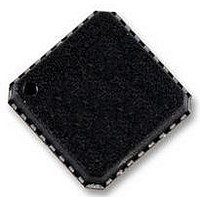
AD7194BCPZ Analog Devices Inc, AD7194BCPZ Datasheet - Page 40

AD7194BCPZ
Manufacturer Part Number
AD7194BCPZ
Description
IC ADC 24BIT SPI 4.8K 32-LFCSP
Manufacturer
Analog Devices Inc
Datasheet
1.AD7194BCPZ.pdf
(56 pages)
Specifications of AD7194BCPZ
Data Interface
DSP, MICROWIRE™, QSPI™, Serial, SPI™
Number Of Bits
24
Sampling Rate (per Second)
4.8k
Number Of Converters
1
Voltage Supply Source
Analog and Digital
Operating Temperature
-40°C ~ 105°C
Mounting Type
Surface Mount
Package / Case
32-WFQFN, CSP Exposed Pad
Resolution (bits)
24bit
Input Channel Type
Pseudo Differential
Supply Voltage Range - Analogue
3V To 5.25V
Supply Voltage Range - Digital
2.7V To 5.25V
Supply
RoHS Compliant
Sampling Rate
4.8kSPS
Rohs Compliant
Yes
Lead Free Status / RoHS Status
Lead free / RoHS Compliant
Other names
AD7194BRUZ
AD7194BRUZ
AD7194BRUZ
Available stocks
Company
Part Number
Manufacturer
Quantity
Price
Part Number:
AD7194BCPZ
Manufacturer:
ADI/亚德诺
Quantity:
20 000
AD7194
When the analog input is constant or a channel change occurs,
valid conversions are available at a constant output data rate.
When conversions are being performed on a single channel and
a step change occurs on the analog input, the ADC continues to
output fully settled conversions if the step change is synchronized
with the conversion process. If the step change is asynchronous,
one conversion is output from the ADC, which is not completely
settled (see Figure 30).
Table 29 shows examples of output data rate and the corres-
ponding FS values.
Table 29. Examples of Output Data Rates and the
Corresponding Settling Time (Zero Latency)
FS[9:0]
480
96
80
Sinc
Figure 31 shows the frequency response of the sinc
FS[9:0] is set to 96 and the master clock is 4.92 MHz. With zero
latency disabled, the output data rate is equal to 50 Hz. With
zero latency enabled, the output data rate is 12.5 Hz. The sinc
filter provides 50 Hz (±1 Hz) rejection in excess of 120 dB
minimum, assuming a stable master clock.
ANALOG
OUTPUT
INPUT
4
ADC
–100
–110
–120
50 Hz/60 Hz Rejection
–10
–20
–30
–40
–50
–60
–70
–80
–90
0
0
Output Data Rate (Hz)
2.5
12.5
15
Figure 31. Sinc
Figure 30. Sinc
25
50
4
Filter Response (FS[9:0] = 96)
FREQUENCY (Hz)
4
1/
Zero Latency Operation
f
ADC
75
100
Settling Time (ms)
400
80
66.6
125
4
filter when
SETTLED
FULLY
150
Rev. 0 | Page 40 of 56
4
Figure 32 shows the frequency response when FS[9:0] is
programmed to 80 and the master clock is equal to 4.92 MHz.
The output data rate is 60 Hz when zero latency is disabled and
15 Hz when zero latency is enabled. The sinc
60 Hz (±1 Hz) rejection of 120 dB minimum, assuming a stable
master clock.
Simultaneous 50 Hz and 60 Hz rejection is obtained when
FS[9:0] is programmed to 480 and the master clock equals
4.92 MHz. The output data rate is 10 Hz when zero latency is
disabled and 2.5 Hz when zero latency is enabled. The sinc
filter provides 50 Hz (±1 Hz) and 60 Hz (±1 Hz) rejection of
120 dB minimum, assuming a stable master clock.
Simultaneous 50 Hz/60 Hz rejection can also be achieved using
the REJ60 bit in the mode register. When FS[9:0] is set to 96
and REJ60 is set to 1, notches are placed at 50 Hz and 60 Hz.
–100
–110
–120
–100
–120
–110
–10
–20
–30
–40
–50
–60
–70
–80
–90
–10
–20
–30
–40
–50
–60
–70
–80
–90
0
0
0
0
Figure 33. Sinc
Figure 32. Sinc
30
30
4
4
Filter Response (FS[9:0] = 480)
Filter Response (FS[9:0] = 80)
FREQUENCY (Hz)
FREQUENCY (Hz)
60
60
90
90
4
filter provides
120
120
150
150
4


