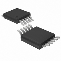
LTC1865IMS#PBF Linear Technology, LTC1865IMS#PBF Datasheet - Page 10

LTC1865IMS#PBF
Manufacturer Part Number
LTC1865IMS#PBF
Description
IC A/D CONV 2CH 16BIT 10-MSOP
Manufacturer
Linear Technology
Datasheet
1.LTC1865CS8PBF.pdf
(24 pages)
Specifications of LTC1865IMS#PBF
Number Of Bits
16
Sampling Rate (per Second)
250k
Data Interface
MICROWIRE™, Serial, SPI™
Number Of Converters
1
Power Dissipation (max)
400mW
Voltage Supply Source
Single Supply
Operating Temperature
-40°C ~ 85°C
Mounting Type
Surface Mount
Package / Case
10-TFSOP, 10-MSOP (0.118", 3.00mm Width)
Resolution (bits)
16bit
Sampling Rate
250kSPS
Input Channel Type
Differential
Supply Voltage Range - Analogue
4.75V To 5.25V
Supply Current
850µA
Rohs Compliant
Yes
Number Of Elements
1
Resolution
16Bit
Architecture
SAR
Sample Rate
250KSPS
Input Polarity
Unipolar
Input Type
Voltage
Rated Input Volt
5V
Differential Input
Yes
Power Supply Requirement
Single
Single Supply Voltage (typ)
5V
Single Supply Voltage (min)
4.75V
Single Supply Voltage (max)
5.25V
Dual Supply Voltage (typ)
Not RequiredV
Dual Supply Voltage (min)
Not RequiredV
Dual Supply Voltage (max)
Not RequiredV
Power Dissipation
400mW
Differential Linearity Error
2LSB(Typ)
Integral Nonlinearity Error
±8LSB
Operating Temp Range
-40C to 85C
Operating Temperature Classification
Industrial
Mounting
Surface Mount
Pin Count
10
Package Type
MSOP
Lead Free Status / RoHS Status
Lead free / RoHS Compliant
Available stocks
Company
Part Number
Manufacturer
Quantity
Price
PIN FUNCTIONS
LTC1864/LTC1865
LTC1864
V
the span of the A/D converter and must be kept free of
noise with respect to GND.
IN
be free of noise with respect to GND.
GND (Pin 4): Analog Ground. GND should be tied directly
to an analog ground plane.
CONV (Pin 5): Convert Input. A logic high on this input
starts the A/D conversion process. If the CONV input is
left high after the A/D conversion is fi nished, the part
LTC1865 (MSOP Package)
CONV (Pin 1): Convert Input. A logic high on this input
starts the A/D conversion process. If the CONV input is
left high after the A/D conversion is fi nished, the part
powers down. A logic low on this input enables the SDO
pin, allowing the data to be shifted out.
CH0, CH1 (Pins 2, 3): Analog Inputs. These inputs must
be free of noise with respect to AGND.
AGND (Pin 4): Analog Ground. AGND should be tied directly
to an analog ground plane.
DGND (Pin 5): Digital Ground. DGND should be tied directly
to an analog ground plane.
SDI (Pin 6): Digital Data Input. The A/D confi guration
word is shifted into this input.
LTC1865 (SO-8 Package)
CONV (Pin 1): Convert Input. A logic high on this input
starts the A/D conversion process. If the CONV input is
left high after the A/D conversion is fi nished, the part
powers down. A logic low on this input enables the SDO
pin, allowing the data to be shifted out.
CH0, CH1 (Pins 2, 3): Analog Inputs. These inputs must
be free of noise with respect to GND.
GND (Pin 4): Analog Ground. GND should be tied directly
to an analog ground plane.
10
REF
+
, IN
(Pin 1): Reference Input. The reference input defi nes
–
(Pins 2, 3): Analog Inputs. These inputs must
powers down. A logic low on this input enables the SDO
pin, allowing the data to be shifted out.
SDO (Pin 6): Digital Data Output. The A/D conversion
result is shifted out of this pin.
SCK (Pin 7): Shift Clock Input. This clock synchronizes
the serial data transfer.
V
free of noise and ripple by bypassing directly to the
analog ground plane.
SDO (Pin 7): Digital Data Output. The A/D conversion
result is shifted out of this output.
SCK (Pin 8): Shift Clock Input. This clock synchronizes
the serial data transfer.
V
free of noise and ripple by bypassing directly to the
analog ground plane.
V
the span of the A/D converter and must be kept free of
noise with respect to AGND.
SDI (Pin 5): Digital Data Input. The A/D confi guration
word is shifted into this input.
SDO (Pin 6): Digital Data Output. The A/D conversion
result is shifted out of this output.
SCK (Pin 7): Shift Clock Input. This clock synchronizes
the serial data transfer.
V
free of noise and ripple by bypassing directly to the analog
ground plane. V
CC
CC
REF
CC
(Pin 8): Positive Supply. This supply must be kept
(Pin 9): Positive Supply. This supply must be kept
(Pin 8): Positive Supply. This supply must be kept
(Pin 10): Reference Input. The reference input defi nes
REF
is tied internally to this pin.
18645fb


