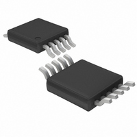
LTC1865CMS#PBF Linear Technology, LTC1865CMS#PBF Datasheet - Page 15

LTC1865CMS#PBF
Manufacturer Part Number
LTC1865CMS#PBF
Description
IC A/D CONV 2CH 16BIT 10-MSOP
Manufacturer
Linear Technology
Datasheet
1.LTC1865CS8PBF.pdf
(24 pages)
Specifications of LTC1865CMS#PBF
Number Of Bits
16
Sampling Rate (per Second)
250k
Data Interface
MICROWIRE™, Serial, SPI™
Number Of Converters
1
Power Dissipation (max)
400mW
Voltage Supply Source
Single Supply
Operating Temperature
0°C ~ 70°C
Mounting Type
Surface Mount
Package / Case
10-TFSOP, 10-MSOP (0.118", 3.00mm Width)
Number Of Elements
1
Resolution
16Bit
Architecture
SAR
Sample Rate
250KSPS
Input Polarity
Unipolar
Input Type
Voltage
Rated Input Volt
5V
Differential Input
Yes
Power Supply Requirement
Single
Single Supply Voltage (typ)
5V
Single Supply Voltage (min)
4.75V
Single Supply Voltage (max)
5.25V
Dual Supply Voltage (typ)
Not RequiredV
Dual Supply Voltage (min)
Not RequiredV
Dual Supply Voltage (max)
Not RequiredV
Power Dissipation
400mW
Differential Linearity Error
2LSB(Typ)
Integral Nonlinearity Error
±8LSB
Operating Temp Range
0C to 70C
Operating Temperature Classification
Commercial
Mounting
Surface Mount
Pin Count
10
Package Type
MSOP
Lead Free Status / RoHS Status
Lead free / RoHS Compliant
Available stocks
Company
Part Number
Manufacturer
Quantity
Price
APPLICATIONS INFORMATION
GENERAL ANALOG CONSIDERATIONS
Grounding
The LTC1864/LTC1865 should be used with an analog
ground plane and single point grounding techniques. Do not
use wire wrapping techniques to breadboard and evaluate
the device. To achieve the optimum performance, use a
printed circuit board. The ground pins (AGND and DGND
for the LTC1865 MSOP package and GND for the LTC1864
and LTC1865 SO-8 package) should be tied directly to the
analog ground plane with minimum lead length.
Bypassing
For good performance, the V
of noise and ripple. Any changes in the V
with respect to ground during the conversion cycle can
1 1 1 1 1 1 1 1 1 1 1 1 1 1 1 1
1 1 1 1 1 1 1 1 1 1 1 1 1 1 1 0
0 0 0 0 0 0 0 0 0 0 0 0 0 0 0 1
0 0 0 0 0 0 0 0 0 0 0 0 0 0 0 0
CC
and V
REF
•
•
•
pins must be free
CC
/V
Figure 5. LTC1865 Transfer Curve
REF
*V
(SELECTED “–” CHANNEL)
REFER TO TABLE 1
IN
= (SELECTED “+” CHANNEL) –
voltage
induce errors or noise in the output code. Bypass the V
and V
a minimum of 1μF tantalum. Keep the bypass capacitor
leads as short as possible.
Analog Inputs
Because of the capacitive redistribution A/D conversion
techniques used, the analog inputs of the LTC1864/LTC1865
have capacitive switching input current spikes. These cur-
rent spikes settle quickly and do not cause a problem if
source resistances are less than 200Ω or high speed op
amps are used (e.g., the LT
LT1630, LT1226 or LT1215). But if large source resistances
are used, or if slow settling op amps drive the inputs, take
care to ensure the transients caused by the current spikes
settle completely before the conversion begins.
REF
pins directly to the analog ground plane with
LTC1864/LTC1865
18645 F05
®
1211, LT1469, LT1807, LT1810,
V
IN
*
15
18645fb
CC


