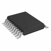
AD7707BRU Analog Devices Inc, AD7707BRU Datasheet - Page 17

AD7707BRU
Manufacturer Part Number
AD7707BRU
Description
IC ADC 16BIT 3CH 20-TSSOP
Manufacturer
Analog Devices Inc
Datasheet
1.AD7707BRUZ-REEL.pdf
(52 pages)
Specifications of AD7707BRU
Rohs Status
RoHS non-compliant
Number Of Bits
16
Sampling Rate (per Second)
500
Data Interface
DSP, MICROWIRE™, QSPI™, Serial, SPI™
Number Of Converters
1
Power Dissipation (max)
1mW
Voltage Supply Source
Analog and Digital
Operating Temperature
-40°C ~ 85°C
Mounting Type
Surface Mount
Package / Case
20-TSSOP (0.173", 4.40mm Width)
Available stocks
Company
Part Number
Manufacturer
Quantity
Price
Company:
Part Number:
AD7707BRUZ
Manufacturer:
ADI
Quantity:
1 000
Part Number:
AD7707BRUZ
Manufacturer:
ADI/亚德诺
Quantity:
20 000
Company:
Part Number:
AD7707BRUZ-REEL7
Manufacturer:
ADI
Quantity:
1 000
OUTPUT NOISE FOR HIGH LEVEL INPUT CHANNEL
AIN3 (3 V OPERATION)
Table 13 shows the AD7707 output rms noise and peak-to-peak
resolution for the selectable notch and −3 dB frequencies for the
part, as selected by FS0, FS1, and FS2 of the clock register. The
numbers given are for the ±5 V, 0 V to 5 V and 0 V to 10 V
ranges with a V
AGND, and AV
generated at an analog input voltage of 0 V for unbuffered mode
of operation. The ±5 V, 0 V to 5 V, and 0 V to 10 V operating
ranges are only achievable in unbuffered mode when operating
at 3 V due to common-mode limitations on the input amplifier.
It is important to note that these numbers represent the
resolution for which there are no code flicker. They are not
calculated based on rms noise but on peak-to-peak noise.
Operating at a gain of 1 in unipolar mode provides a range of
Table 13. Output RMS Noise/Peak-to-Peak Resolution vs. Gain and Output Update Rate @ +3 V AIN3 Unbuffered Mode Only
Filter First Notch
and Output
Data Rate
MCLK IN = 2.4576 MHz
10 Hz
50 Hz
60 Hz
250 Hz
500 Hz
MCLK IN = 1 MHz
4.05 Hz
20 Hz
25 Hz
100 Hz
200 Hz
REF
DD
= 3 V. These numbers are typical and are
of 1.225 V, VBIAS = 1.225 V, HICOM =
−3 dB
Frequency
2.62 Hz
13.1 Hz
15.72 Hz
65.5 Hz
131 Hz
1.06 Hz
5.24 Hz
6.55 Hz
26.2 Hz
52.4 Hz
RMS Noise
(μV)
12.4
30.35
34.55
498
2266
13.9
32.2
33.4
430
2207
0 V to 10 V Range
P-P (Bits)
Resolution
16
16
16
12.5
10.5
16
16
16
13
10.5
Rev. B | Page 17 of 52
RMS Noise
(μV)
7.02
16.4
19.13
204
1151
7.3
17.4
18.57
200
1048
0 V to +10 V. Operating the high level channel with a gain of 2
in bipolar mode provides a ±5 V operating range. Operating at
a gain of 2 in unipolar mode provides an operating range of 0 V
to 5 V. The output noise comes from two sources. The first is
the electrical noise in the semiconductor devices (device noise)
used in the implementation of the modulator. Secondly, when
the analog input is converted into the digital domain, quantiza-
tion noise is added. The device noise is at a low level and is
independent of frequency. The quantization noise starts at an
even lower level but rises rapidly with increasing frequency to
become the dominant noise source. The numbers in Table 13
are given for the bipolar input ranges. For the unipolar ranges,
the rms noise numbers are the same as the bipolar range, but
the peak-to-peak resolution is now based on half the signal
range, which effectively means losing 1 bit of resolution.
±5 V Range
P-P (Bits)
Resolution
16
16
16
13
10.5
16
16
16
13
10.5
RMS Noise
(μV)
7.02
16.4
19.13
204
1151
7.3
17.4
18.57
200
1048
0 to 5 V Range
P-P (Bits)
Resolution
16
15.5
15
12
9.5
16
15
15
12
9.5
AD7707


