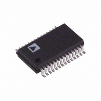
AD7854ARS Analog Devices Inc, AD7854ARS Datasheet - Page 25

AD7854ARS
Manufacturer Part Number
AD7854ARS
Description
IC ADC 12BIT PARALLEL LP 28-SSOP
Manufacturer
Analog Devices Inc
Datasheet
1.AD7854LARZ.pdf
(28 pages)
Specifications of AD7854ARS
Rohs Status
RoHS non-compliant
Number Of Bits
12
Sampling Rate (per Second)
200k
Data Interface
Parallel
Number Of Converters
2
Power Dissipation (max)
30mW
Voltage Supply Source
Analog and Digital
Operating Temperature
-40°C ~ 85°C
Mounting Type
Surface Mount
Package / Case
28-SSOP (0.200", 5.30mm Width)
Available stocks
Company
Part Number
Manufacturer
Quantity
Price
Part Number:
AD7854ARSZ
Manufacturer:
ADI/亚德诺
Quantity:
20 000
REV. B
AD7854/AD7854L to TMS320C30
Figure 40 shows a parallel interface between the AD7854/
AD7854L and the TMS320C3x family of DSPs. The
AD7854/AD7854L is interfaced to the Expansion Bus of the
TMS320C3x. Two wait states are required in this interface.
These can be programmed using the WTCNT bits of the
Expansion Bus Control register (see TMS320C3x Users Guide
for details). Data from the AD7854/AD7854L can be read
using the following instruction:
Data can be loaded into the AD7854/AD7854L using the
instructions:
where ARn is an auxiliary register containing the lower 16 bits
of the address of the AD7854/AD7854L in the TMS320C3x
memory space, Rx is the register into which the ADC data is
loaded during a load operation, Ry contains the 8 LSBs of
data and Rz contains the 8 MSBs of data to be written to the
AD7854/AD7854L.
Figure 40. AD7854/AD7854L to TMS320C30 Parallel
Interface
LDI *ARn,Rx
STI Ry,*ARn++
STI Rz,*ARn--
*ADDITIONAL PINS OMITTED FOR CLARITY
TMS320C30*
XA12–XA1
XD23–XD0
IOSTRB
XR/W
INTx
XA0
EXPANSION ADDRESS BUS
EXPANSION DATA BUS
DECODE
ADDR
CS
RD
BUSY
DB11–DB0
HBEN
WR
AD7854/
AD7854L*
–25–
AD7854/AD7854L to DSP5600x
Figure 41 shows a parallel interface between the AD7854/
AD7854L and the DSP5600x series of DSPs. The AD7854/
AD7854L should be mapped into the top 64 locations of Y data
memory. If extra wait states are needed in this interface, they
can be programmed using the Port A bus control register (please
see DSP5600x User’s Manual for details). Data can be read
from the DSP5600x using the following instruction:
Data can be written to the AD7854/AD7854L using the follow-
ing two instructions:
Where ADCaddr is the address in the DSP5600x address space
to which the AD7854/AD7854L has been mapped.
Figure 41. AD7854/AD7854L to DSP5600x Parallel Interface
MOVE Y:ADCaddr, X 0
MOVE X0, Y:ADCaddr
MOVE X1, Y:ADCaddr+1
*ADDITIONAL PINS OMITTED FOR CLARITY
DSP56000/
DSP56002*
D23–D0
A15–A1
IRQ
WR
X/Y
DS
RD
A0
ADDRESS BUS
DECODE
DATA BUS
ADDR
AD7854/AD7854L
CS
HBEN
WR
RD
BUSY
DB11–DB0
AD7854/
AD7854L*


