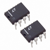
LTC1291DCN8#PBF Linear Technology, LTC1291DCN8#PBF Datasheet - Page 5

LTC1291DCN8#PBF
Manufacturer Part Number
LTC1291DCN8#PBF
Description
IC DATA ACQ SYSTEM 12BIT 8-DIP
Manufacturer
Linear Technology
Type
Data Acquisition System (DAS)r
Datasheet
1.LTC1291DCN8PBF.pdf
(20 pages)
Specifications of LTC1291DCN8#PBF
Resolution (bits)
12 b
Data Interface
Serial, Parallel
Voltage Supply Source
Single Supply
Voltage - Supply
5V
Operating Temperature
0°C ~ 70°C
Mounting Type
Through Hole
Package / Case
8-DIP (0.300", 7.62mm)
Number Of Elements
1
Resolution
12Bit
Architecture
SAR
Sample Rate
54KSPS
Input Polarity
Unipolar
Input Type
Voltage
Rated Input Volt
5V
Differential Input
Yes
Power Supply Requirement
Single
Single Supply Voltage (typ)
5V
Dual Supply Voltage (typ)
Not RequiredV
Dual Supply Voltage (min)
Not RequiredV
Dual Supply Voltage (max)
Not RequiredV
Power Dissipation
500mW
Differential Linearity Error
±1LSB(Typ)
Integral Nonlinearity Error
±0.75LSB
Operating Temp Range
0C to 70C
Operating Temperature Classification
Commercial
Mounting
Through Hole
Pin Count
8
Package Type
PDIP N
Lead Free Status / RoHS Status
Lead free / RoHS Compliant
Sampling Rate (per Second)
-
Lead Free Status / Rohs Status
Compliant
Available stocks
Company
Part Number
Manufacturer
Quantity
Price
PI FU CTIO S
TYPICAL PERFOR
CS (Pin 1): Chip Select Input. A logic low on this input
enables the LTC1291.
CH0, CH1 (Pins 2, 3): Analog Inputs. These inputs must
be free of noise with respect to GND.
GND (Pin 4): Analog Ground. GND should be tied directly
to an analog ground plane.
D
shifted into this input.
IN
100
250
200
100
150
10
U
50
1
(Pin 5): Digital Data Input. The multiplexer address is
0
100
–50
D
Sample-and-Hold Acquisition
Time vs Source Resistance
V
T
0V TO 5V INPUT STEP
OUT
V
A
CC
CC
MSB-FIRST DATA
–25
= 25 C
= 5V
= 5V
Delay Time vs Temperature
V
U
AMBIENT TEMPERATURE ( C)
IN
R
0
SOURCE
R
SOURCE
25
+
+
–
1k
LSB-FIRST DATA
U
+ ( )
50
75
W
100
A
1291 G13
1291 G10
U
10k
125
CE
C
1000
HARA TERISTICS
600
900
800
700
500
400
300
200
100
1.0
0.6
0.4
0.2
0.8
0
0
100
–50
Maximum Clock Rate vs Source
Resistance
Input Channel Leakage Current
vs Temperature
–30
–10
AMBIENT TEMPERATURE ( C)
C
1k
10
R
SOURCE –
30
D
result is shifted out of this output.
CLK (Pin 7): Shift Clock. This clock synchronizes the serial
data transfer.
V
This pin provides power and defines the span of the A/D
converter. This supply must be kept free of noise and
ripple by bypassing directly to the analog ground plane.
OFF CHANNEL
50
R
CC
OUT
SOURCE
+V
( )
(V
IN
ON CHANNEL
GUARANTEED
10k
70
(Pin 6): Digital Data Output. The A/D conversion
REF
V
CLK = 1MHz
–
CC
+
–
90 110
= 5V
+IN
–IN
) (Pin 8): Positive Supply and Reference Voltage.
1291 G11
1291 G14
100k
130
* MAXIMUM CLK FREQUENCY REPRESENTS THE CLK
**MAXIMUM R
FREQUENCY AT WHICH A 0.1LSB SHIFT IN THE
ERROR AT ANY CODE TRANSITION FROM ITS 1MHz
VALUE IS FIRST DETECTED
VALUE AT WHICH A 0.1LSB CHANGE IN FULL SCALE
ERROR FROM ITS VALUE AT R
DETECTED
100
10k
1k
10
1
10
Maximum Filter Resistor vs
Cycle Time
C
FILTER
FILTER
+V
IN
REPRESENTS THE FILTER RESISTOR
R
FILTER
1 F
100
CYCLE TIME ( s)
FILTER
+
–
LTC1291
= 0 IS FIRST
1k
1291 G12
1291fa
5
10k


