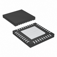
MAX1020BETX+ Maxim Integrated Products, MAX1020BETX+ Datasheet - Page 18

MAX1020BETX+
Manufacturer Part Number
MAX1020BETX+
Description
IC ADC/DAC 10BIT 36-TQFN-EP
Manufacturer
Maxim Integrated Products
Type
ADC, DACr
Datasheet
1.MAX1020BETX.pdf
(44 pages)
Specifications of MAX1020BETX+
Resolution (bits)
10 b
Sampling Rate (per Second)
225k
Data Interface
MICROWIRE™, QSPI™, Serial, SPI™
Voltage Supply Source
Analog and Digital
Voltage - Supply
4.75 V ~ 5.25 V
Operating Temperature
-40°C ~ 85°C
Mounting Type
Surface Mount
Package / Case
36-TQFN Exposed Pad
Lead Free Status / RoHS Status
Lead free / RoHS Compliant
10-Bit, Multichannel ADCs/DACs with FIFO,
Temperature Sensing, and GPIO Ports
The MAX1020/MAX1022/MAX1057/MAX1058 integrate
a multichannel, 10-bit ADC and an octal, 10-bit DAC in
a single IC. These devices also include a temperature
sensor and configurable GPIOs with a 25MHz SPI-/
QSPI-/MICROWIRE-compatible serial interface. The
ADC is available in 8/12/16 input-channel versions. The
octal DAC outputs settle within 2.0µs, and the ADC has
a 225ksps conversion rate.
All devices include an internal reference (2.5V or
4.096V) providing a well-regulated, low-noise reference
for both the ADC and DAC. Programmable reference
modes for the ADC and DAC allow the use of an inter-
nal reference, an external reference, or a combination
of both. Features such as an internal ±1°C accurate
temperature sensor, FIFO, scan modes, programmable
internal or external clock modes, data averaging, and
AutoShutdown allow users to minimize both power con-
sumption and processor requirements. The low glitch
energy (4nV
the integrated octal DACs make these devices ideal for
digital control of fast-response closed-loop systems.
The devices are guaranteed to operate with a supply
voltage from +2.7V to +3.6V (MAX1057) and from
+4.5V to +5.5V (MAX1020/MAX1022/MAX1058), they
consume 25mA at 225ksps throughput, only 22µA at
1ksps throughput, and under 0.2µA in the shutdown
mode. The MAX1057/MAX1058 feature 12 GPIOs, while
the MAX1020 offers four GPIOs that can be configured
as inputs or outputs.
Figure 1 shows the MAX1057/MAX1058 functional dia-
gram. The MAX1020 only includes the GPIOA0, GPIOA1
and GPIOC0, GPIOC1 block. The MAX1022 excludes
the GPIOs. The output-conditioning circuitry takes the
internal parallel data bus and converts it to a serial data
format at DOUT, with the appropriate wake-up timing.
The arithmetic logic unit (ALU) performs the averaging
function.
The MAX1020/MAX1022/MAX1057/MAX1058 feature a
serial interface that is compatible with SPI and
MICROWIRE devices. For SPI, ensure the SPI bus mas-
ter (typically a microcontroller (µC)) runs in master
mode so that it generates the serial clock signal. Select
the SCLK frequency of 25MHz or less, and set the
clock polarity (CPOL) and phase (CPHA) in the µC con-
trol registers to the same value. The MAX1020/
MAX1022/MAX1057/MAX1058 operate with SCLK idling
high or low, and thus operate with CPOL = CPHA = 0 or
18
______________________________________________________________________________________
•
s) and low digital feedthrough (0.5nV
SPI-Compatible Serial Interface
Detailed Description
•
s) of
CPOL = CPHA = 1. Set CS low to latch any input data
at DIN on the falling edge of SCLK. Output data at
DOUT is updated on the falling edge of SCLK in clock
modes 00, 01, and 10. Output data at DOUT is updated
on the rising edge of SCLK in clock mode 11. See
Figures 6–11. Bipolar true-differential results and tem-
perature-sensor results are available in two’s comple-
ment format, while all other results are in binary.
A high-to-low transition on CS initiates the data-input
operation. Serial communications to the ADC always
begin with an 8-bit command byte (MSB first) loaded
from DIN. The command byte and the subsequent data
bytes are clocked from DIN into the serial interface on
the falling edge of SCLK. The serial-interface and fast-
interface circuitry is common to the ADC, DAC, and
GPIO sections. The content of the command byte
determines whether the SPI port should expect 8, 16, or
24 bits and whether the data is intended for the ADC,
DAC, or GPIOs (if applicable). See Table 1. Driving CS
high resets the serial interface.
The conversion register controls ADC channel selec-
tion, ADC scan mode, and temperature-measurement
requests. See Table 4 for information on writing to the
conversion register. The setup register controls the
clock mode, reference, and unipolar/bipolar ADC con-
figuration. Use a second byte, following the first, to
write to the unipolar-mode or bipolar-mode registers.
See Table 5 for details of the setup register and see
Tables 6, 7, and 8 for setting the unipolar- and bipolar-
mode registers. Hold CS low between the command
byte and the second and third byte. The ADC averag-
ing register is specific to the ADC. See Table 9 to
address that register. Table 11 shows the details of the
reset register.
Begin a write to the DAC by writing 0001XXXX as a
command byte. The last 4 bits of this command byte
are don’t-care bits. Write another 2 bytes (holding CS
low) to the DAC interface register following the com-
mand byte to select the appropriate DAC and the data
to be written to it. See the DAC Serial Interface section
and Tables 10, 20, and 21.
Write to the GPIOs (if applicable) by issuing a com-
mand byte to the appropriate register. Writing to the
MAX1020 GPIOs requires 1 additional byte following
the command byte. Writing to the MAX1057/
MAX1058 requires 2 additional bytes following the com-
mand byte. See Tables 12–19 for details on GPIO con-
figuration, writes, and reads. See the GPIO Command
section. Command bytes written to the GPIOs on
devices without GPIOs are ignored.


