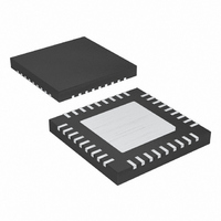
MAX1020BETX+ Maxim Integrated Products, MAX1020BETX+ Datasheet - Page 22

MAX1020BETX+
Manufacturer Part Number
MAX1020BETX+
Description
IC ADC/DAC 10BIT 36-TQFN-EP
Manufacturer
Maxim Integrated Products
Type
ADC, DACr
Datasheet
1.MAX1020BETX.pdf
(44 pages)
Specifications of MAX1020BETX+
Resolution (bits)
10 b
Sampling Rate (per Second)
225k
Data Interface
MICROWIRE™, QSPI™, Serial, SPI™
Voltage Supply Source
Analog and Digital
Voltage - Supply
4.75 V ~ 5.25 V
Operating Temperature
-40°C ~ 85°C
Mounting Type
Surface Mount
Package / Case
36-TQFN Exposed Pad
Lead Free Status / RoHS Status
Lead free / RoHS Compliant
10-Bit, Multichannel ADCs/DACs with FIFO,
Temperature Sensing, and GPIO Ports
The first 2 bytes of data read out after a temperature
measurement always contain the 12-bit temperature
result, preceded by four leading zeros, MSB first. If
another temperature measurement is performed before
the first temperature result is read out, the old measure-
ment is overwritten by the new result. Temperature
results are in degrees Celsius (two’s complement), at a
resolution of 8 LSB per degree. See the Temperature
Measurements section for details on converting the dig-
ital code to a temperature.
In addition to the 10-bit ADC, the MAX1020/MAX1022/
MAX1057/MAX1058 also include eight voltage-output,
10-bit, monotonic DACs with less than 4 LSB integral
nonlinearity error and less than 1 LSB differential nonlin-
earity error. Each DAC has a 2µs settling time and ultra-
low glitch energy (4nV
unipolar binary with 1 LSB = V
Figure 1 shows the functional diagram of the MAX1057/
MAX1058. The shift register converts a serial 16-bit word
to parallel data for each input register operating with a
clock rate up to 25MHz. The SPI-compatible digital inter-
face to the shift register consists of CS, SCLK, DIN, and
DOUT. Serial data at DIN is loaded on the falling edge
of SCLK. Pull CS low to begin a write sequence. Begin a
write to the DAC by writing 0001XXXX as a command
byte. The last 4 bits of the DAC select register are don’t-
care bits. See Table 10. Write another 2 bytes to the
DAC interface register following the command byte to
select the appropriate DAC and the data to be written to
it. See Tables 20 and 21.
The eight double-buffered DACs include an input and a
DAC register. The input registers are directly connect-
ed to the shift register and hold the result of the most
recent write operation. The eight 10-bit DAC registers
hold the current output code for the respective DAC.
Data can be transferred from the input registers to the
DAC registers by pulling LDAC low or by writing the
appropriate DAC command sequence at DIN. See
Table 20. The outputs of the DACs are buffered through
eight rail-to-rail op amps.
The MAX1020/MAX1022/MAX1057/MAX1058 DAC out-
put-voltage range is based on the internal reference or
an external reference. Write to the setup register (see
Table 5) to program the reference. If using an external
voltage reference, bypass REF1 with a 0.1µF capacitor
to AGND. The MAX1057 internal reference is 2.5V. The
MAX1020/MAX1022/MAX1058 internal reference is
22
______________________________________________________________________________________
•
s). The 10-bit DAC code is
REF
DAC Digital Interface
/ 4096.
10-Bit DAC
4.096V. When using an external reference on any of
these devices, the voltage range is 0.7V to AV
See Table 2 for various analog outputs from the DAC.
The state of the RES_SEL input determines the wake-up
state of the DAC outputs. Connect RES_SEL to AV
AGND upon power-up to be sure the DAC outputs
wake up to a known state. Connect RES_SEL to AGND
to wake up all DAC outputs at 000h. While RES_SEL is
low, the 100kΩ internal resistor pulls the DAC outputs to
AGND and the output buffers are powered down.
Connect RES_SEL to AV
at 3FFh. While RES_SEL is high, the 100kΩ pullup
resistor pulls the DAC outputs to V
buffers are powered down.
See Table 21 for a description of the DAC power-up
and power-down modes.
In addition to the internal ADC and DAC, the
MAX1057/MAX1058 also provide 12 general-purpose
input/output channels, GPIOA0–GPIOA3, GPIOB0–
GPIOB3, and GPIOC0–GPIOC3. The MAX1020 includes
four GPIO channels (GPIOA0, GPIOA1, GPIOC0,
Table 2. DAC Output Code Table
MSB
11
10
10
01
00
00
DAC CONTENTS
1111
0000
0000
0111
0000
0000
1111
0001
0000
0111
0001
0000
LSB
DAC Power-On Wake-Up Modes
DD
to wake up all DAC outputs
+
V
DAC Transfer Function
REF
ANALOG OUTPUT
DAC Power-Up Modes
+
+
+
+
⎛
⎜
⎝
REF1
V
V
V
V
1024
REF
REF
REF
512
REF
and the output
⎛
⎜
⎝
⎛
⎜
⎝
⎛
⎜
⎝
⎛
⎜
⎝
⎞
⎟ =
⎠
1024
1023
1024
1024
1024
0
513
511
1
⎛
⎜
⎝
DD
+
⎞
⎟
⎠
⎞
⎟
⎠
⎞
⎟
⎠
⎞
⎟
⎠
GPIOs
V
.
2
REF
DD
⎞
⎟
⎠
or


