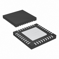
MAX1020BETX+ Maxim Integrated Products, MAX1020BETX+ Datasheet - Page 23

MAX1020BETX+
Manufacturer Part Number
MAX1020BETX+
Description
IC ADC/DAC 10BIT 36-TQFN-EP
Manufacturer
Maxim Integrated Products
Type
ADC, DACr
Datasheet
1.MAX1020BETX.pdf
(44 pages)
Specifications of MAX1020BETX+
Resolution (bits)
10 b
Sampling Rate (per Second)
225k
Data Interface
MICROWIRE™, QSPI™, Serial, SPI™
Voltage Supply Source
Analog and Digital
Voltage - Supply
4.75 V ~ 5.25 V
Operating Temperature
-40°C ~ 85°C
Mounting Type
Surface Mount
Package / Case
36-TQFN Exposed Pad
Lead Free Status / RoHS Status
Lead free / RoHS Compliant
GPIOC1). Read and write to the GPIOs as detailed in
Table 1 and Tables 12–19. Also, see the GPIO Command
section. See Figures 11 and 12 for GPIO timing.
Write to the GPIOs by writing a command byte to the
GPIO command register. Write a single data byte to the
MAX1020 following the command byte. Write 2 bytes to
the MAX1057/MAX1058 following the command byte.
The GPIOs can sink and source current. The
MAX1057/MAX1058 GPIOA0–GPIOA3 can sink and
source up to 15mA. GPIOB0–GPIOB3 and GPIOC0–
GPIOC3 can sink 4mA and source 2mA. The MAX1020
GPIOA0 and GPIOA1 can sink and source up to 15mA.
The MAX1020 GPIOC0 and GPIOC1 can sink 4mA and
source 2mA. See Table 3.
The MAX1020/MAX1022/MAX1057/MAX1058 can oper-
ate from an internal oscillator. The internal oscillator is
active in clock modes 00, 01, and 10. Figures 6, 7, and
8 show how to start an ADC conversion in the three
internally timed conversion modes.
Read out the data at clock speeds up to 25MHz
through the SPI interface.
Set CKSEL1 and CKSEL0 in the setup register to 11 to
set up the interface for external clock mode 11. See
Table 5. Pulse SCLK at speeds from 0.1MHz to
3.6MHz. Write to SCLK with a 40% to 60% duty cycle.
The SCLK frequency controls the conversion timing.
See Figure 9 for clock mode 11 timing. See the ADC
Conversions in Clock Mode 11 section.
Address the reference through the setup register, bits 3
and 2. See Table 5. Following a wake-up delay, set
REFSEL[1:0] = 00 to program both the ADC and DAC
for internal reference use. Set REFSEL[1:0] = 10 to pro-
gram the ADC for internal reference. Set REFSEL[1:0] =
10 to program the DAC for external reference, REF1.
When using REF1 or REF2/AIN_ in external-reference
mode, connect a 0.1µF capacitor to AGND. Set REF-
SEL[1:0] = 01 to program the ADC and DAC for exter-
nal-reference mode. The DAC uses REF1 as its external
reference, while the ADC uses REF2 as its external ref-
Table 3. GPIO Maximum Sink/Source Current
CURRENT
SOURCE
SINK
10-Bit, Multichannel ADCs/DACs with FIFO,
______________________________________________________________________________________
GPIOA0–GPIOA3
Temperature Sensing, and GPIO Ports
ADC/DAC References
15
15
MAX1057/MAX1058 (mA)
Clock Modes
External Clock
Internal Clock
GPIOB0–GPIOB3
4
2
erence. Set REFSEL[1:0] = 11 to program the ADC for
external differential reference mode. REF1 is the posi-
tive reference and REF2 is the negative reference in the
ADC external differential mode.
When REFSEL [1:0] = 00 or 10, REF2/AIN_ functions as
an analog input channel. When REFSEL [1:0] = 01 or 11,
REF2/AIN_ functions as the device’s negative reference.
Issue a command byte setting bit 0 of the conversion
register to one to take a temperature measurement. See
Table
MAX1058 perform temperature measurements with an
internal diode-connected transistor. The diode bias cur-
rent changes from 68µA to 4µA to produce a tempera-
ture-dependent bias voltage difference. The second
conversion result at 4µA is subtracted from the first at
68µA to calculate a digital value that is proportional to
absolute temperature. The output data appearing at
DOUT is the digital code above, minus an offset to
adjust from Kelvin to Celsius.
The reference voltage used for the temperature mea-
surements is always derived from the internal reference
source to ensure that 1 LSB corresponds to 1/8 of a
degree Celsius. On every scan where a temperature
measurement is requested, the temperature conversion
is carried out first. The first 2 bytes of data read from
the FIFO contain the result of the temperature measure-
ment. If another temperature measurement is per-
formed before the first temperature result is read out,
the old measurement is overwritten by the new result.
Temperature results are in degrees Celsius (two’s com-
plement). See the Applications Information section for
information on how to perform temperature measure-
ments in each clock mode.
The MAX1020/MAX1022/MAX1057/MAX1058 communi-
cate between the internal registers and the external cir-
cuitry through the SPI-compatible serial interface. Table
1 details the command byte, the registers, and the bit
names. Tables 4–12 show the various functions within
the conversion register, setup register, unipolar-mode
register, bipolar-mode register, ADC averaging regis-
ter, DAC select register, reset register, and GPIO com-
mand register, respectively.
GPIOC0–GPIOC3
4
2
4.
The
Temperature Measurements
GPIOA0, GPIOA1
MAX1020/MAX1022/MAX1057/
15
15
Register Descriptions
MAX1020 (mA)
GPIOC0, GPIOC1
4
2
23


