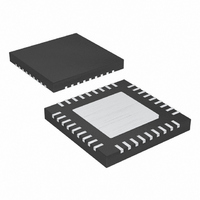
MAX1020BETX+ Maxim Integrated Products, MAX1020BETX+ Datasheet - Page 29

MAX1020BETX+
Manufacturer Part Number
MAX1020BETX+
Description
IC ADC/DAC 10BIT 36-TQFN-EP
Manufacturer
Maxim Integrated Products
Type
ADC, DACr
Datasheet
1.MAX1020BETX.pdf
(44 pages)
Specifications of MAX1020BETX+
Resolution (bits)
10 b
Sampling Rate (per Second)
225k
Data Interface
MICROWIRE™, QSPI™, Serial, SPI™
Voltage Supply Source
Analog and Digital
Voltage - Supply
4.75 V ~ 5.25 V
Operating Temperature
-40°C ~ 85°C
Mounting Type
Surface Mount
Package / Case
36-TQFN Exposed Pad
Lead Free Status / RoHS Status
Lead free / RoHS Compliant
disables averaging. For example, if AVGON = 1,
NAVG[1:0] = 00, NSCAN[1:0] = 11 and SCAN[1:0] =
10, 16 results are written to the FIFO, with each result
being the average of four conversions of channel N.
Write a command byte 0001XXXX to the DAC select
register (as shown in Table 9) to set up the DAC inter-
face and indicate that another word will follow. The last
4 bits of the DAC select register are don’t-care bits. The
word that follows the DAC select-register command
byte controls the DAC serial interface. See Table 20
and the DAC Serial Interface section.
Write to the reset register (as shown in Table 11) to
clear the FIFO or reset all registers (excluding the DAC
and GPIO registers) to their default states. When the
Table 10. DAC Select Register
Table 11. Reset Register
FBGON
RESET
NAME
SLOW
NAME
BIT
BIT
—
—
—
—
—
—
—
—
—
X
X
X
X
7 (MSB) Set to zero to select ADC reset register.
0 (LSB)
7 (MSB) Set to zero to select DAC select register.
BIT
10-Bit, Multichannel ADCs/DACs with FIFO,
6
5
4
3
2
1
BIT
6
5
4
3
2
1
0
______________________________________________________________________________________
Set to zero to select ADC reset register.
Set to zero to select ADC reset register.
Set to zero to select ADC reset register.
Set to one to select ADC reset register.
Set to zero to clear the FIFO only. Set to
one to set the device in its power-on
condition.
Set to one to turn on slow mode.
Set to one to force internal bias block and
bandgap reference to be always powered
up.
Set to zero to select DAC select register.
Set to zero to select DAC select register.
Set to one to select DAC select register.
Don’t care.
Don’t care.
Don’t care.
Don’t care.
Temperature Sensing, and GPIO Ports
FUNCTION
FUNCTION
DAC Select Register
Reset Register
RESET bit in the reset register is set to 0, the FIFO is
cleared. Set the RESET bit to one to return all the
device registers to their default power-up state. All reg-
isters power up in state 00000000, except for the setup
register that powers up in clock mode 10 (CKSEL1 = 1
and REFSEL1 = 1). The DAC and GPIO registers are
not reset by writing to the reset register. Set the SLOW
bit to one to add a 15ns delay in the DOUT signal path
to provide a longer hold time. Writing a one to the
SLOW bit also clears the contents of the FIFO. Set the
FBGON bit to one to force the bias block and bandgap
reference to power up regardless of the state of the
DAC and activity of the ADC block. Setting the FBGON
bit high also removes the programmed wake-up delay
between conversions in clock modes 01 and 11.
Setting the FBGON bit high also clears the FIFO.
Write a command byte to the GPIO command register
to configure, write, or read the GPIOs, as detailed in
Table 12.
Write the command byte 00000011 to configure the
GPIOs. The eight SCLK cycles following the command
byte load data from DIN to the GPIO configuration reg-
ister in the MAX1020. The 16 SCLK cycles following the
command byte load data from DIN to the GPIO configu-
ration register in the MAX1057/MAX1058. See Tables
13 and 14. The register bits are updated after the last
Table 12. GPIO Command Register
GPIOSEL1
BIT NAME
GPIOSEL1
GPIOSEL2
—
—
—
—
—
—
1
1
0
GPIOSEL2
7 (MSB)
0 (LSB)
BIT
6
5
4
3
2
1
1
0
1
Set to zero to select GPIO register.
Set to zero to select GPIO register.
Set to zero to select GPIO register.
Set to zero to select GPIO register.
Set to zero to select GPIO register.
Set to zero to select GPIO register.
GPIO configuration bit.
GPIO write bit.
GPIO configuration; written data is
entered in the GPIO configuration
register.
GPIO write; written data is entered
in the GPIO write register.
GPIO read; the next 8/16 SCLK
cycles transfer the state of all GPIO
drivers into DOUT.
FUNCTION
FUNCTION
GPIO Command
29


