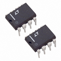
LTC1291BCN8 Linear Technology, LTC1291BCN8 Datasheet - Page 14

LTC1291BCN8
Manufacturer Part Number
LTC1291BCN8
Description
IC DATA ACQ SYSTEM 12BIT 8-DIP
Manufacturer
Linear Technology
Type
Data Acquisition System (DAS)r
Datasheet
1.LTC1291DCN8PBF.pdf
(20 pages)
Specifications of LTC1291BCN8
Resolution (bits)
12 b
Data Interface
Serial, Parallel
Voltage Supply Source
Single Supply
Voltage - Supply
5V
Operating Temperature
0°C ~ 70°C
Mounting Type
Through Hole
Package / Case
8-DIP (0.300", 7.62mm)
Lead Free Status / RoHS Status
Contains lead / RoHS non-compliant
Sampling Rate (per Second)
-
Available stocks
Company
Part Number
Manufacturer
Quantity
Price
Company:
Part Number:
LTC1291BCN8
Manufacturer:
LINEAR
Quantity:
5 479
Part Number:
LTC1291BCN8
Manufacturer:
LT/凌特
Quantity:
20 000
Part Number:
LTC1291BCN8#PBF
Manufacturer:
LINEAR/凌特
Quantity:
20 000
LTC1291
ANALOG CONSIDERATIONS
Grounding
The LTC1291 should be used with an analog ground plane
and single point grounding techniques. Do not use wire
wrapping techniques to breadboard and evaluate the device.
To achieve the optimum performance, use a PC board. The
ground pin (Pin 4) should be tied directly to the ground
plane with minimum lead length. Figure 4 shows an
example of an ideal LTC1291 ground plane for a two-sided
board. Of course this much ground plane will not always
be possible, but users should strive to get as close to this
ideal as possible.
Bypassing
For good performance, V
ripple. Any changes in the V
ground during the conversion cycle can induce error or
noise in the output code. V
below 0.5mV by bypassing the V
analog ground plane with a minimum of 22 F tantalum
capacitor and with leads as short as possible. A 0.1 F
ceramic disk capacitor should also be placed directly
across V
possible. The V
impedance such as that obtained from a voltage regulator
(e.g., LT323A). Figures 5 and 6 show the effects of good
and poor V
14
A
PPLICATI
Figure 4. Example Ground Plane for the LTC1291
CC
ANALOG GROUND
CC
(Pin 8) and GND (Pin 4) as close to the pins as
PLANE
bypassing.
O
CC
U
supply should have a low output
S
1
2
3
4
TANTALUM
I FOR ATIO
CC
CC
U
0.1 F
LTC1291
22 F
noise and ripple can be kept
must be free of noise and
CC
voltage with respect to
LTC1291 F04
8
6
5
7
CC
V
W
CC
pin directly to the
U
Analog Inputs
Because of the capacitive redistribution A/D conversion
techniques used, the analog inputs of the LTC1291 have
capacitive switching input current spikes. These current
spikes settle quickly and do not cause a problem. If large
source resistances are used or if slow settling op amps
drive the inputs, take care to insure the transients caused
by the current spikes settle completely before the
conversion begins.
Minimizing Gain and Offset Error
Because the LTC1291’s reference is taken from the power
supply pin (V
bypassing is important for attaining the best performance
from the A/D converter. Any parasitic resistance in the V
Figure 5. Poor V
Ripple Can Cause A/D Errors
Figure 6. Good V
Noise and Ripple on V
CC
), proper PC board layout and supply
HORIZONTAL: 10 s/DIV
HORIZONTAL: 10 s/DIV
CC
CC
Bypassing. Noise and
Bypassing Keeps
CC
Below 1mV
CS
V
CC
1291fa
CC


