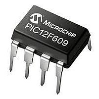
MCP14E8-E/P Microchip Technology, MCP14E8-E/P Datasheet - Page 13

MCP14E8-E/P
Manufacturer Part Number
MCP14E8-E/P
Description
3A MOSFET Driver 8 PDIP .300in TUBE
Manufacturer
Microchip Technology
Datasheet
1.MCP14E8-EP.pdf
(30 pages)
Specifications of MCP14E8-E/P
Leaded Process Compatible
Yes
Rohs Compliant
Yes
Peak Reflow Compatible (260 C)
Yes
Module Configuration
Low Side
Peak Output Current
2A
Output Resistance
5ohm
Input Delay
45ns
Output Delay
45ns
Supply Voltage Range
4.5V To 18V
Driver Case Style
DIP
No. Of Pins
8
Available stocks
Company
Part Number
Manufacturer
Quantity
Price
Company:
Part Number:
MCP14E8-E/P
Manufacturer:
MICROCHIP
Quantity:
12 000
4.0
4.1
MOSFET drivers are high-speed, high-current devices
which are intended to source/sink high-peak currents to
charge/discharge the gate capacitance of external
MOSFETs, or insulated gate bipolar transistors
(IGBTs). In high-frequency switching power supplies,
the Pulse-Width Modulation (PWM) controller may not
have the drive capability to directly drive the power
MOSFET. MOSFET drivers, like the MCP14E6/7/8
family, can be used to provide additional source/sink
current capability.
An additional degree of control has been added to the
MCP14E6/7/8 family. There are seperate enable func-
tions for each driver that allow for the immediate termi-
nation of the output pulse, regardless of the state of the
input signal.
4.2
The ability of a MOSFET driver to transition from a fully
OFF state to a fully ON state are characterized by the
drivers’ rise time (t
delays (t
can typically charge and discharge a 1000 pF load
capacitance, in approximately 12 ns, along with a typical
matched propagation delay of 45 ns.
Figure 4-2
used to verify the MCP14E6/7/8 timing.
FIGURE 4-1:
Waveform.
© 2011 Microchip Technology Inc.
Output
Input
+5V
18V
0V
0V
Input
Input
D1
APPLICATION INFORMATION
General Information
MOSFET Driver Timing
10%
and t
show the test circuit and timing waveform
D2
90%
½ MCP14E8
). The MCP14E6/7/8 family of drivers
V
t
MCP14E6
D1
R
DD
10%
), fall time (t
Inverting Driver Timing
= 18V
t
F
1 µF
F
C
C
) and propagation
L
L
t
D2
0.1 µF
Ceramic
Output
Output
= 1000 pF
= 1000 pF
Figure 4-1
90%
t
10%
R
90%
and
FIGURE 4-2:
Waveform
4.3
The ENB_A and ENB_B enable pins allow the indepen-
dent control of OUT A and OUT B, respectively. They
are active-high and are internally pulled up to V
that the default state is to enable the driver. These pins
can be left floating for normal operation.
When an enable pin voltage is above enable pin high
threshold voltage, (V
and allowed to react to changes in the INPUT pin volt-
age state. Similarly, when the enable pin voltage falls
below the enable pin low threshold voltage, (V
that driver output is disabled and does not respond to
the changes in the INPUT pin voltage state. When the
driver is disabled, the output goes to a low state. Refer
to
of the enable function are compatible with logic levels.
Hysteresis is provided to help increase the noise immu-
nity of the enable function, avoiding false triggers of the
enable signal during driver switching. For robust
designs, it is recommended that the slew rate of the
enable pin signal be greater than 1V/ns.
There are propagation delays associated with the
driver receiving an enable signal and the output
reacting. These propagation delays, t
graphically represented in
Output
Input
Table 4-1
+5V
18V
0V
0V
Input
Input
Enable Function
10%
for enable pin logic. The threshold voltages
V
½ MCP14E8
t
D1
MCP14E6
DD
MCP14E6/7/8
EN_H
90%
= 18V
Non-Inverting Driver Timing
10%
), that driver output is enabled
Figure
1 µF
t
R
4-3.
C
C
DS25006A-page 13
L
L
0.1 µF
Ceramic
Output
Output
= 1000 pF
= 1000 pF
t
90%
D3
D
2
10%
and t
90%
D4
EN_L
DD
, are
t
so
F
),


