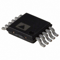
AD5312BRMZ Analog Devices Inc, AD5312BRMZ Datasheet

AD5312BRMZ
Specifications of AD5312BRMZ
Available stocks
Related parts for AD5312BRMZ
AD5312BRMZ Summary of contents
Page 1
FEATURES AD5302: Two 8-bit buffered DACs in 1 package A version: ±1 LSB INL, B version: ±0.5 LSB INL AD5312: Two 10-bit buffered DACs in 1 package A version: ±4 LSB INL, B version: ±2 LSB INL AD5322: Two 12-bit ...
Page 2
AD5302/AD5312/AD5322 TABLE OF CONTENTS Features .............................................................................................. 1 Applications....................................................................................... 1 General Description ......................................................................... 1 Functional Block Diagram .............................................................. 1 Revision History ............................................................................... 2 Specifications..................................................................................... 3 AC Specifications.......................................................................... 4 Timing Characteristics ................................................................ 5 Absolute Maximum Ratings............................................................ 7 ESD Caution.................................................................................. 7 Pin Configuration ...
Page 3
SPECIFICATIONS kΩ to GND REF L Table 1. A Version 2 Parameter Min Typ PERFORMANCE AD5302 Resolution 8 Relative Accuracy ...
Page 4
AD5302/AD5312/AD5322 A Version 2 Parameter Min Typ POWER REQUIREMENTS V 2 (Normal Mode 4 5.5 V 300 2 3.6 V 230 DD I (Full Power-Down ...
Page 5
TIMING CHARACTERISTICS 5.5 V, all specifications T DD Table 3. Parameter Limit at T MIN 4 ...
Page 6
AD5302/AD5312/AD5322 OUTPUT IDEAL VOLTAGE ACTUAL POSITIVE OFFSET DAC CODE ERROR DEADBAND AMPLIFIER FOOTROOM (1mV) NEGATIVE OFFSET ERROR Figure 3. Transfer Function with Negative Offset OFFSET ERROR ACTUAL OUTPUT VOLTAGE IDEAL POSITIVE OFFSET ERROR DAC CODE Figure 4. Transfer Function with ...
Page 7
ABSOLUTE MAXIMUM RATINGS 25°C, unless otherwise noted. A Table 4. Parameter Rating V to GND –0 Digital Input Voltage to GND –0 Reference Input Voltage to –0 ...
Page 8
AD5302/AD5312/AD5322 PIN CONFIGURATION AND FUNCTION DESCRIPTIONS Table 5. Pin Function Descriptions Pin No. Mnemonic Description 1 LDAC Active Low Control Input. This pin transfers the contents of the input registers to their respective DAC registers. Pulsing LDAC low allows either ...
Page 9
TERMINOLOGY Relative Accuracy For the DAC, relative accuracy or integral nonlinearity (INL measure of the maximum deviation, in LSB, from a straight line passing through the actual endpoints of the DAC transfer function. A typical INL vs. code ...
Page 10
AD5302/AD5312/AD5322 TYPICAL PERFORMANCE CHARACTERISTICS 1 25° 0.5 0 –0.5 –1 100 150 CODE Figure 6. AD5302 Typical INL Plot 25° ...
Page 11
MAX INL MAX DNL 0 MIN DNL –0.25 MIN INL –0.50 –0.75 –1. (V) REF Figure 12. AD5302 INL and DNL Error vs ...
Page 12
AD5302/AD5312/AD5322 600 BOTH DACS IN GAIN-OF-TWO MODE REFERENCE INPUTS BUFFERED 500 400 –40°C 300 +105°C 200 100 0 2.5 3.0 3.5 4.0 V (V) DD Figure 18. Supply Current vs. Supply Voltage 1.0 BOTH DACS IN THREE-STATE CONDITION 0.8 0.6 ...
Page 13
Figure 24. AD5322 Major-Code Transition 10 0 –10 –20 –30 –40 –50 –60 10 100 1k 10k 100k FREQUENCY(Hz) Figure 25. Multiplying Bandwidth (Small-Signal Frequency Response) 1 0.5 0 –0.5 ...
Page 14
AD5302/AD5312/AD5322 FUNCTIONAL DESCRIPTION The AD5302/AD5312/AD5322 are dual resistor-string DACs fabricated on a CMOS process with resolutions of 8, 10, and 12 bits, respectively. They contain reference buffers and output buffer amplifiers, and are written to via a 3-wire serial interface. ...
Page 15
SERIAL INTERFACE The AD5302/AD5312/AD5322 are controlled over a versatile, 3-wire serial interface, which operates at clock rates MHz and is compatible with SPI, QSPI, MICROWIRE, and DSP interface standards. INPUT SHIFT REGISTER The input shift register is ...
Page 16
AD5302/AD5312/AD5322 POWER-DOWN MODES The AD5302/AD5312/AD5322 have very low power consump- tion, dissipating only 0.7 mW with supply and 1.5 mW with supply. Power consumption can be further reduced when the DACs are not in ...
Page 17
MICROPROCESSOR INTERFACING AD5302/AD5312/AD5322 TO ADSP-2101/ADSP- 2103 INTERFACE Figure 34 shows a serial interface between the AD5302/AD5312/ AD5322 and the ADSP-2101/ADSP-2103. The 2103 should be set up to operate in the SPORT transmit alternate framing mode. The ADSP-2101/ADSP-2103 through the SPORT ...
Page 18
AD5302/AD5312/AD5322 APPLICATIONS INFORMATION TYPICAL APPLICATION CIRCUIT The AD5302/AD5312/AD5322 can be used with a wide range of reference voltages, especially if the reference inputs are configured to be unbuffered, in which case the devices offer full, one-quadrant multiplying capability over a ...
Page 19
OPTO-ISOLATED INTERFACE FOR PROCESS CONTROL APPLICATIONS Each AD5302/AD5312/AD5322 has a versatile 3-wire serial interface, making them ideal for generating accurate voltages in process control and industrial applications. Due to noise, safety requirements, or distance, it can be necessary to isolate ...
Page 20
AD5302/AD5312/AD5322 COARSE AND FINE ADJUSTMENT USING THE AD5302/AD5312/AD5322 The DACs in the AD5302/AD5312/AD5322 can be paired together to form a coarse and fine adjustment function, as shown in Figure 44. DAC A is used to provide the coarse adjustment while ...
Page 21
... AD5312BRM-REEL −40°C to +105°C AD5312BRM-REEL7 −40°C to +105°C 1 AD5312BRMZ −40°C to +105°C 1 AD5312BRMZ-REEL −40°C to +105°C 1 AD5312BRMZ-REEL7 −40°C to +105°C AD5322ARM −40°C to +105°C AD5322ARM-REEL7 −40°C to +105°C 1 AD5322ARMZ −40°C to +105°C 1 AD5322ARMZ-REEL7 − ...
Page 22
AD5302/AD5312/AD5322 NOTES Rev Page ...
Page 23
NOTES AD5302/AD5312/AD5322 Rev Page ...
Page 24
AD5302/AD5312/AD5322 NOTES ©2006 Analog Devices, Inc. All rights reserved. Trademarks and registered trademarks are the property of their respective owners. C00928-0-4/06(C) Rev Page ...


