AD9708ARZ Analog Devices Inc, AD9708ARZ Datasheet
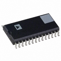
IC DAC 8BIT 100MSPS 28-SOIC

AD9708ARZ

Manufacturer Part Number
AD9708ARZ
Description
IC DAC 8BIT 100MSPS 28-SOIC
Manufacturer
Analog Devices Inc
Series
TxDAC®r
Datasheet

Specifications of AD9708ARZ

Data Interface
Parallel
Settling Time
35ns
Number Of Bits
8
Number Of Converters
1
Voltage Supply Source
Analog and Digital
Power Dissipation (max)
175mW
Operating Temperature
-40°C ~ 85°C
Mounting Type
Surface Mount
Package / Case
28-SOIC (7.5mm Width)
Resolution (bits)
8bit
Sampling Rate
125MSPS
Input Channel Type
Parallel
Supply Voltage Range - Analog
2.7V To 5.5V
Supply Voltage Range - Digital
2.7V To 5.5V
Package
28SOIC W
Resolution
8 Bit
Conversion Rate
125 MSPS
Architecture
Segment
Digital Interface Type
Parallel
Number Of Outputs Per Chip
1
Output Type
Current
Full Scale Error
±10 %FSR
Integral Nonlinearity Error
±0.5 LSB
Maximum Settling Time
0.035(Typ) us
Lead Free Status / RoHS Status
Lead free / RoHS Compliant
For Use With
AD9708-EBZ - BOARD EVAL FOR AD9708
Lead Free Status / RoHS Status
Lead free / RoHS Compliant, Lead free / RoHS Compliant

Available stocks

Company
Part Number
Manufacturer
Quantity
Price
Part Number:
AD9708ARZ
Manufacturer:
ADI/亚德诺
Quantity:
20 000
a
PRODUCT DESCRIPTION
The AD9708 is the 8-bit resolution member of the TxDAC
series of high performance, low power CMOS digital-to-analog
converters (DACs). The TxDAC family, which consists of pin
compatible 8-, 10-, 12-, and 14-bit DACs, was specifically opti-
mized for the transmit signal path of communication systems. All
of the devices share the same interface options, small outline
package and pinout, thus providing an upward or downward
component selection path based on performance, resolution and
cost. The AD9708 offers exceptional ac and dc performance
while supporting update rates up to 125 MSPS.
The AD9708’s flexible single-supply operating range of +2.7 V
to +5.5 V and low power dissipation are well suited for portable
and low power applications. Its power dissipation can be
further reduced to 45 mW, without a significant degradation in
performance, by lowering the full-scale current output. In addi-
tion, a power-down mode reduces the standby power dissipa-
tion to approximately 20 mW.
The AD9708 is manufactured on an advanced CMOS process.
A segmented current source architecture is combined with a
proprietary switching technique to reduce spurious components
and enhance dynamic performance. Edge-triggered input latches
and a temperature compensated bandgap reference have been inte-
grated to provide a complete monolithic DAC solution. Flexible
supply options support +3 V and +5 V CMOS logic families.
The AD9708 is a current-output DAC with a nominal full-scale
output current of 20 mA and > 100 k output impedance.
TxDAC is a registered trademark of Analog Devices, Inc.
REV. B
Information furnished by Analog Devices is believed to be accurate and
reliable. However, no responsibility is assumed by Analog Devices for its
use, nor for any infringements of patents or other rights of third parties
which may result from its use. No license is granted by implication or
otherwise under any patent or patent rights of Analog Devices.
FEATURES
Member of Pin-Compatible TxDAC Product Family
125 MSPS Update Rate
8-Bit Resolution
Linearity: 1/4 LSB DNL
Linearity:
Differential Current Outputs
SINAD @ 5 MHz Output: 50 dB
Power Dissipation: 175 mW @ 5 V to 45 mW @ 3 V
Power-Down Mode: 20 mW @ 5 V
On-Chip 1.20 V Reference
Single +5 V or +3 V Supply Operation
Packages: 28-Lead SOIC and 28-Lead TSSOP
Edge-Triggered Latches
Fast Settling: 35 ns Full-Scale Settling to 0.1%
APPLICATIONS
Communications
Signal Reconstruction
Instrumentation
1/4 LSB INL
One Technology Way, P.O. Box 9106, Norwood, MA 02062-9106, U.S.A.
Tel: 781/329-4700
Fax: 781/326-8703
Differential current outputs are provided to support single-
ended or differential applications. The current outputs may be
directly tied to an output resistor to provide two complemen-
tary, single-ended voltage outputs. The output voltage compliance
range is 1.25 V.
The AD9708 contains a 1.2 V on-chip reference and reference
control amplifier, which allows the full-scale output current to
be simply set by a single resistor. The AD9708 can be driven by
a variety of external reference voltages. The AD9708’s full-scale
current can be adjusted over a 2 mA to 20 mA range without
any degradation in dynamic performance. Thus, the AD9708
may operate at reduced power levels or be adjusted over a 20 dB
range to provide additional gain ranging capabilities.
The AD9708 is available in 28-lead SOIC and 28-lead TSSOP
packages. It is specified for operation over the industrial tem-
perature range.
PRODUCT HIGHLIGHTS
1. The AD9708 is a member of the TxDAC product family, which
2. Manufactured on a CMOS process, the AD9708 uses a pro-
3. On-chip, edge-triggered input CMOS latches readily interface
4. A flexible single-supply operating range of +2.7 V to +5.5 V
5. A temperature compensated, 1.20 V bandgap reference is
6. The current output(s) of the AD9708 can easily be config-
provides an upward or downward component selection path
based on resolution (8 to 14 bits), performance and cost.
prietary switching technique that enhances dynamic perfor-
mance well beyond 8- and 10-bit video DACs.
to +3 V and +5 V CMOS logic families. The AD9708 can
support update rates up to 125 MSPS.
and a wide full-scale current adjustment span of 2 mA to
20 mA allows the AD9708 to operate at reduced power levels
(i.e., 45 mW) without any degradation in dynamic performance.
included on-chip providing a complete DAC solution. An
external reference may be used.
ured for various single-ended or differential applications.
CLOCK
R
SET
+5V
0.1 F
FUNCTIONAL BLOCK DIAGRAM
REF IO
FS ADJ
CLOCK
DVDD
DCOM
+1.20V REF
TxDAC
SLEEP
REFLO
World Wide Web Site: http://www.analog.com
COMP1
DIGITAL DATA INPUTS (DB7–DB0)
8-Bit, 100 MSPS+
50pF
®
0.1 F
D/A Converter
CURRENT
SEGMENTED
SOURCE
SWITCHES
ARRAY
LATCHES
© Analog Devices, Inc., 1999
+5V
AVDD
AD9708
AD9708
ACOM
COMP2
IOUTA
IOUTB
0.1 F

Related parts for AD9708ARZ

AD9708ARZ Summary of contents

Page 1

FEATURES Member of Pin-Compatible TxDAC Product Family 125 MSPS Update Rate 8-Bit Resolution Linearity: 1/4 LSB DNL Linearity: 1/4 LSB INL Differential Current Outputs SINAD @ 5 MHz Output Power Dissipation: 175 ...

Page 2

AD9708–SPECIFICATIONS DC SPECIFICATIONS ( MIN Parameter RESOLUTION MONOTONICITY 1 DC ACCURACY Integral Linearity Error (INL) Differential Nonlinearity (DNL) ANALOG OUTPUT Offset Error Gain Error (Without Internal Reference) Gain Error (With Internal Reference) 2 Full-Scale Output Current Output Compliance ...

Page 3

DYNAMIC SPECIFICATIONS P arameter DYNAMIC PERFORMANCE Maximum Output Update Rate (f CLOCK 1 Output Settling Time (t ) (to 0.1%) ST Output Propagation Delay ( Glitch Impulse 1 Output Rise Time (10% to 90%) 1 Output Fall Time ...

Page 4

AD9708 ABSOLUTE MAXIMUM RATINGS* With Parameter Respect to Min AVDD ACOM –0.3 DVDD DCOM –0.3 ACOM DCOM –0.3 AVDD DVDD –6.5 CLOCK, SLEEP DCOM –0.3 Digital Inputs DCOM –0.3 IOUTA, IOUTB ACOM –1.0 COMP1, COMP2 ACOM –0.3 REFIO, FSADJ ACOM ...

Page 5

DEFINITIONS OF SPECIFICATIONS Linearity Error (Also Called Integral Nonlinearity or INL) Linearity error is defined as the maximum deviation of the actual analog output from the ideal output, determined by a straight line drawn from zero to full scale. Differential ...

Page 6

AD9708 Typical AC Characterization Curves Single-Ended Output mA, T OUTA OUTFS A 70 THD @ 50MSPS THD @ 10MSPS 65 THD @ 100MSPS SINAD @ 10MSPS SINAD @ 50MSPS 45 SINAD @ ...

Page 7

FUNCTIONAL DESCRIPTION Figure 12 shows a simplified block diagram of the AD9708. The AD9708 consists of a large PMOS current source array capable of providing total current. The array is divided into 31 equal currents ...

Page 8

AD9708 OPTIONAL EXTERNAL REF BUFFER REFLO +1.2V REF REFIO ADDITIONAL FS ADJ LOAD 0 AD9708 Figure 13. Internal Reference Configuration The internal reference can be disabled by connecting REFLO to AVDD. In this case, an external reference may ...

Page 9

Figure 17 shows a buffered singled-ended output con- figuration in which the op amp, U1, performs an I-V conversion on the AD9708 output current. U1 provides a negative unipolar output voltage and its full-scale output voltage is simply the ...

Page 10

AD9708 – mA OUTFS Figure 19. I vs. I AVDD OUTFS POWER DISSIPATION The power dissipation the AD9708 is ...

Page 11

The necessity and value of this resistor will be dependent upon the logic family used. For a more detailed discussion of the implementation and construction of high speed, mixed signal printed circuit boards, refer to Analog Devices’ ...

Page 12

AD9708 Figure 26. Evaluation Board Schematic –12– REV. B ...

Page 13

REV. B Figure 27. Silkscreen Layer—Top Figure 28. Component Side PCB Layout (Layer 1) –13– AD9708 ...

Page 14

AD9708 Figure 29. Ground Plane PCB Layout (Layer 2) Figure 30. Power Plane PCB Layout (Layer 3) –14– REV. B ...

Page 15

REV. B Figure 31. Solder Side PCB Layout (Layer 4) Figure 32. Silkscreen Layer—Bottom –15– AD9708 ...

Page 16

AD9708 PIN 1 0.0118 (0.30) 0.0040 (0.10) 0.006 (0.15) 0.002 (0.05) SEATING PLANE OUTLINE DIMENSIONS Dimensions shown in inches and (mm). 28-Lead, 300 Mil SOIC (R-28) 0.7125 (18.10) 0.6969 (17.70 0.2992 (7.60) 0.2914 (7.40) 0.4193 (10.65 ...

Related keywords