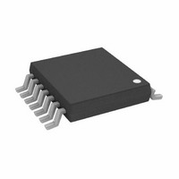
AD5625BRUZ Analog Devices Inc, AD5625BRUZ Datasheet - Page 31

AD5625BRUZ
Manufacturer Part Number
AD5625BRUZ
Description
IC DAC NANO 12BIT QUAD 14-TSSOP
Manufacturer
Analog Devices Inc
Series
nanoDAC™r
Specifications of AD5625BRUZ
Data Interface
I²C, Serial
Settling Time
3µs
Number Of Bits
12
Number Of Converters
4
Voltage Supply Source
Single Supply
Operating Temperature
-40°C ~ 105°C
Mounting Type
Surface Mount
Package / Case
14-TSSOP
Resolution (bits)
12bit
Sampling Rate
333kSPS
Input Channel Type
Serial
Supply Voltage Range - Analogue
2.7V To 5.5V
Supply Current
1.9mA
Digital Ic Case Style
TSSOP
No.
RoHS Compliant
Number Of Channels
4
Resolution
12b
Conversion Rate
333KSPS
Interface Type
Serial (2-Wire/I2C)
Single Supply Voltage (typ)
3.3/5V
Dual Supply Voltage (typ)
Not RequiredV
Architecture
Resistor-String
Power Supply Requirement
Single
Output Type
Voltage
Single Supply Voltage (min)
2.7V
Single Supply Voltage (max)
5.5V
Dual Supply Voltage (min)
Not RequiredV
Dual Supply Voltage (max)
Not RequiredV
Operating Temp Range
-40C to 105C
Operating Temperature Classification
Industrial
Mounting
Surface Mount
Pin Count
14
Lead Free Status / RoHS Status
Lead free / RoHS Compliant
Power Dissipation (max)
-
Lead Free Status / Rohs Status
Compliant
APPLICATIONS INFORMATION
USING A REFERENCE AS A POWER SUPPLY FOR
THE AD56x5R/AD56x5
Because the supply current required by the AD56x5R/AD56x5 is
extremely low, an alternative option is to use a voltage reference
to supply the required voltage to the part (see Figure 72). This is
especially useful if the power supply is noisy or if the system
supply voltages are at some value other than 5 V or 3 V, for
example, 15 V. The voltage reference outputs a steady supply
voltage for the AD56x5R/AD56x5. If the low dropout REF195 is
used, it must supply 450 μA of current to the AD56x5R/AD56x5
with no load on the output of the DAC. When the DAC output
is loaded, the
The total current required (with a 5 kΩ load on the DAC
output) is
The load regulation of the REF195 is typically 2 ppm/mA,
resulting in a 4 ppm (20 μV) error for the 2 mA current drawn
from it. This corresponds to a 0.263 LSB error.
BIPOLAR OPERATION USING THE
AD56x5R/AD56x5
The AD56x5R/AD56x5 have been designed for single-supply
operation, but a bipolar output range is also possible using the
circuit shown in Figure 73. The circuit gives an output voltage
range of ±5 V. Rail-to-rail operation at the amplifier output is
achievable using an
The output voltage for any input code can be calculated as follows:
where D represents the input code in decimal (0 to 65,535).
If V
This is an output voltage range of ±5 V, with 0x0000 corre-
sponding to a −5 V output and 0xFFFF corresponding to a
+5 V output.
DD
1 mA + (5 V/5 kΩ) = 2 mA
V
V
= 5 V, R1 = R2 = 10 kΩ,
O
O
Figure 72. REF195 as Power Supply to the AD56x5R/AD56x5
INTERFACE
=
=
⎛
⎜
⎝
SERIAL
⎡
⎢
⎣
2-WIRE
V
10
65
DD
REF195
,
×
536
×
D
⎛
⎜
⎝
⎞
⎟
⎠
SDA
SCL
65
AD820
−
REF195
D
,
also must supply the current to the load.
15V
5
536
V
⎞
⎟
⎠
or an
×
5V
AD5625R/
AD5645R/
AD5665R/
AD5625/
⎛
⎜
⎝
AD5665
R1
GND
V
DD
OP295
R1
+
R2
⎞
⎟
⎠
−
as the output amplifier.
V
V
OUT
DD
= 0V TO 5V
×
⎛
⎜
⎝
R2
R1
⎞
⎟
⎠
⎤
⎥
⎦
Rev. B | Page 31 of 36
AD5625R/AD5645R/AD5665R, AD5625/AD5665
POWER SUPPLY BYPASSING AND GROUNDING
When accuracy is important in a circuit, it is helpful to carefully
consider the power supply and ground return layout on the board.
The printed circuit board containing the AD56x5R/AD56x5
should have separate analog and digital sections, each having its
own area of the board. If the AD56x5R/AD56x5 are in a system
where other devices require an AGND-to-DGND connection,
the connection should be made at one point only. This ground
point should be as close as possible to the AD56x5R/AD56x5.
The power supply to the AD56x5R/AD56x5 should be bypassed
with 10 μF and 0.1 μF capacitors. The capacitors should be
located as close as possible to the device, with the 0.1 μF capaci-
tor ideally right up against the device. The 10 μF capacitor is
the tantalum bead type. It is important that the 0.1 μF capacitor
have low effective series resistance (ESR) and low effective
series inductance (ESI), for example, common ceramic types of
capacitors. This 0.1 μF capacitor provides a low impedance path
to ground for high frequencies caused by transient currents due
to internal logic switching.
The power supply line itself should have as large a trace as
possible to provide a low impedance path and to reduce glitch
effects on the supply line. Clocks and other fast switching
digital signals should be shielded from other parts of the board
by digital ground. Avoid crossover of digital and analog signals
if possible. When traces cross on opposite sides of the board,
ensure that they run at right angles to each other to reduce
feedthrough effects through the board. The best board layout
technique is the microstrip technique where the component
side of the board is dedicated to the ground plane only, and the
signal traces are placed on the solder side. However, this is not
always possible with a 2-layer board.
+5V
10µF
Figure 73. Bipolar Operation with the AD56x5R/AD56x5
0.1µF
GND
V
DD
AD5625R/
AD5645R/
AD5665R/
AD5625/
AD5665
R1 = 10kΩ
INTERFACE
SCL
SERIAL
2-WIRE
V
OUT
SDA
AD820/
OP295
R2 = 10kΩ
+5V
–5V
V
±5V
O


