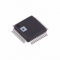
ADV7123JSTZ330 Analog Devices Inc, ADV7123JSTZ330 Datasheet - Page 18

ADV7123JSTZ330
Manufacturer Part Number
ADV7123JSTZ330
Description
IC DAC VIDEO 3CH 330MHZ 48-LQFP
Manufacturer
Analog Devices Inc
Datasheet
1.ADV7123KSTZ50.pdf
(24 pages)
Specifications of ADV7123JSTZ330
Data Interface
Parallel
Settling Time
15ns
Number Of Bits
10
Number Of Converters
3
Voltage Supply Source
Single Supply
Power Dissipation (max)
30mW
Operating Temperature
0°C ~ 70°C
Mounting Type
Surface Mount
Package / Case
48-LQFP
Resolution (bits)
10bit
Sampling Rate
330MSPS
Input Channel Type
Parallel
Supply Current
16mA
Digital Ic Case Style
QFP
No. Of Pins
48
Lead Free Status / RoHS Status
Lead free / RoHS Compliant
Available stocks
Company
Part Number
Manufacturer
Quantity
Price
Company:
Part Number:
ADV7123JSTZ330
Manufacturer:
TOSHIBA
Quantity:
6 219
Company:
Part Number:
ADV7123JSTZ330
Manufacturer:
ADI
Quantity:
210
Company:
Part Number:
ADV7123JSTZ330
Manufacturer:
Analog Devices Inc
Quantity:
10 000
Part Number:
ADV7123JSTZ330
Manufacturer:
ADI/亚德诺
Quantity:
20 000
ADV7123
Table 9. Typical Video Output Truth Table (R
Video Output Level
White Level
Video
Video to BLANK
Black Level
Black to BLANK
BLANK Level
SYNC Level
VIDEO SYNCHRONIZATION AND CONTROL
The ADV7123 has a single composite sync ( SYNC ) input
control. Many graphics processors and CRT controllers have the
ability of generating horizontal sync (HSYNC), vertical sync
(VSYNC), and composite SYNC .
In a graphics system that does not automatically generate a
composite SYNC signal, the inclusion of some additional logic
circuitry enables the generation of a composite SYNC signal.
The sync current is internally connected directly to the IOG
output, thus encoding video synchronization information onto
the green video channel. If it is not required to encode sync
information onto the ADV7123, the SYNC input should be tied
to logic low.
REFERENCE INPUT
The ADV7123 contains an on-board voltage reference. The V
pin is normally terminated to V
Alternatively, the part can, if required, be overdriven by an
external 1.23 V reference (AD1580).
A resistance, R
determines the amplitude of the output video level according to
Equation 1 and Equation 2 for the ADV7123.
Equation 1 applies to the ADV7123 only, when SYNC is being
used. If SYNC is not being encoded onto the green channel,
Equation 1 is similar to Equation 2.
Using a variable value of R
the analog output video levels. Use of a fixed 560 Ω R
yields the analog output levels quoted in the Specifications section.
These values typically correspond to the RS-343A video wave-
form values, as shown in Figure 23.
DACs
The ADV7123 contains three matched 10-bit DACs. The DACs
are designed using an advanced, high speed, segmented architec-
ture. The bit currents corresponding to each digital input are
routed to either the analog output (bit = 1) or GND (bit = 0)
by a sophisticated decoding scheme. Because all this circuitry is
on one monolithic device, matching between the three DACs is
optimized. As well as matching, the use of identical current
IOG (mA) = 11,445 × V
IOR, IOB (mA) = 7989.6 × V
SET
, connected between the R
IOG (mA)
Video + 7.2
Video
7.2
0
7.2
0
SET
26.0
allows for accurate adjustment of
REF
AA
(V)/R
REF
through a 0.1 μF capacitor.
(V)/R
SET
(Ω)
IOG (mA)
0
18.67 − Video
18.67 − Video
18.67
18.67
18.67
18.67
SET
SET
(Ω)
pin and GND,
SET
= 530 Ω, R
SET
resistor
IOR/IOB (mA)
18.67
Video
Video
0
0
0
0
Rev. D | Page 18 of 24
(1)
(2)
REF
LOAD
= 37.5 Ω)
sources in a monolithic design guarantees monotonicity and
low glitch. The on-board operational amplifier stabilizes the
full-scale output current against temperature and power supply
variations.
ANALOG OUTPUTS
The ADV7123 has three analog outputs, corresponding to the
red, green, and blue video signals.
The red, green, and blue analog outputs of the ADV7123 are
high impedance current sources. Each one of these three RGB
current outputs is capable of directly driving a 37.5 Ω load, such
as a doubly terminated 75 Ω coaxial cable. Figure 24 shows
the required configuration for each of the three RGB outputs
connected into a doubly terminated 75 Ω load. This arrangement
develops RS-343A video output voltage levels across a 75 Ω
monitor.
A suggested method of driving RS-170 video levels into a 75 Ω
monitor is shown in Figure 25. The output current levels of the
DACs remain unchanged, but the source termination resistance,
Z
More detailed information regarding load terminations for
various output configurations, including RS-343A and RS-170,
is available in the AN-205 Application Note, Video Formats and
Required Load Terminations, available from Analog Devices, at
www.analog.com.
S
, on each of the three DACs is increased from 75 Ω to 150 Ω.
TERMINATION REPEATED THREE TIMES
TERMINATION REPEATED THREE TIMES
IOR/IOB (mA)
0
18.67 − Video
18.67 − Video
18.67
18.67
18.67
18.67
FOR RED, GREEN, AND BLUE DACs
FOR RED, GREEN, AND BLUE DACs
TERMINATION)
TERMINATION)
DACs
DACs
Z
(SOURCE
(SOURCE
Z
S
Figure 24. Analog Output Termination for RS-343A
S
Figure 25. Analog Output Termination for RS-170
= 150Ω
= 75Ω
IOR, IOG, IOB
IOR, IOG, IOB
SYNC
1
1
0
1
0
1
0
Z
(CABLE)
Z
(CABLE)
0
0
BLANK
1
1
1
1
1
0
0
= 75Ω
= 75Ω
Data
Data
0x000H
DAC Input Data
0x3FFH
0x000H
0xXXXH (don’t care)
0xXXXH (don’t care)
Z
(MONITOR)
Z
(MONITOR)
L
L
= 75Ω
= 75Ω


