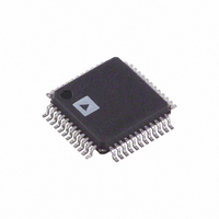
ADV7123JSTZ330 Analog Devices Inc, ADV7123JSTZ330 Datasheet - Page 8

ADV7123JSTZ330
Manufacturer Part Number
ADV7123JSTZ330
Description
IC DAC VIDEO 3CH 330MHZ 48-LQFP
Manufacturer
Analog Devices Inc
Datasheet
1.ADV7123KSTZ50.pdf
(24 pages)
Specifications of ADV7123JSTZ330
Data Interface
Parallel
Settling Time
15ns
Number Of Bits
10
Number Of Converters
3
Voltage Supply Source
Single Supply
Power Dissipation (max)
30mW
Operating Temperature
0°C ~ 70°C
Mounting Type
Surface Mount
Package / Case
48-LQFP
Resolution (bits)
10bit
Sampling Rate
330MSPS
Input Channel Type
Parallel
Supply Current
16mA
Digital Ic Case Style
QFP
No. Of Pins
48
Lead Free Status / RoHS Status
Lead free / RoHS Compliant
Available stocks
Company
Part Number
Manufacturer
Quantity
Price
Company:
Part Number:
ADV7123JSTZ330
Manufacturer:
TOSHIBA
Quantity:
6 219
Company:
Part Number:
ADV7123JSTZ330
Manufacturer:
ADI
Quantity:
210
Company:
Part Number:
ADV7123JSTZ330
Manufacturer:
Analog Devices Inc
Quantity:
10 000
Part Number:
ADV7123JSTZ330
Manufacturer:
ADI/亚德诺
Quantity:
20 000
ADV7123
3.3 V TIMING SPECIFICATIONS
V
Table 6.
Parameter
ANALOG OUTPUTS
CLOCK CONTROL
1
2
3
4
5
6
7
These maximum and minimum specifications are guaranteed over this range.
Temperature range: T
Timing specifications are measured with input levels of 3.0 V (V
Rise time was measured from the 10% to 90% point of zero to full-scale transition, fall time from the 90% to 10% point of a full-scale transition.
Measured from 50% point of full-scale transition to 2% of final value.
Guaranteed by characterization.
f
CLK
AA
Analog Output Delay
Analog Output Rise/Fall Time
Analog Output Transition Time
Analog Output Skew
CLOCK Frequency
Data and Control Setup
Data and Control Hold
CLOCK Period
CLOCK Pulse Width High
CLOCK Pulse Width Low
CLOCK Pulse Width High
CLOCK Pulse Width Low
CLOCK Pulse Width High
CLOCK Pulse Width Low
CLOCK Pulse Width High
CLOCK Pulse Width Low
Pipeline Delay
PSAVE Up Time
maximum specification production tested at 125 MHz; 5 V limits specified here are guaranteed by characterization.
= 3.0 V to 3.6 V,
3
NOTES
1. OUTPUT DELAY (
2. OUTPUT RISE/FALL TIME (
3. TRANSITION TIME (
(R9 TO R0, G9 TO G0, B9 TO B0,
(IOR, IOR, IOG, IOG, IOB, IOB)
OF FULL-SCALE TRANSITION.
FINAL OUTPUT VALUE.
6
6
MIN
7
1
ANALOG OUTPUTS
to T
V
6
DIGITAL INPUTS
REF
SYNC, BLANK)
MAX
6
t
6
= 1.235 V, R
: −40°C to +85°C at 50 MHz and 140 MHz, 0°C to 70°C at 240 MHz and 330 MHz.
6
) MEASURED FROM THE 50% POINT OF THE RISING EDGE OF CLOCK TO THE 50% POINT
t
8
) MEASURED FROM THE 50% POINT OF FULL-SCALE TRANSITION TO WITHIN 2% OF THE
CLOCK
4
5
t
7
) MEASURED BETWEEN THE 10% AND 90% POINTS OF FULL-SCALE TRANSITION.
SET
= 560 Ω, C
t
4
t
3
Symbol
t
t
t
t
f
t
t
t
t
t
t
t
t
t
t
t
t
t
CLK
6
7
8
9
1
2
3
4
5
4
5
4
5
4
5
PD
10
L
IH
) and 0 V (V
t
= 10 pF. All specifications T
5
Figure 2. Timing Diagram
Rev. D | Page 8 of 24
IL
) 0 for both 5 V and 3.3 V supplies.
Min
0.2
1.5
3
1.4
1.4
1.875
1.875
2.85
2.85
8.0
8.0
1.0
t
1
Typ
7.5
1.0
15
1 2
1.0
4
t
2
t
MIN
6
1.0
Max
50
140
240
330
10
to T
MAX
t
8
,
t
2
7
Unit
ns
ns
ns
ns
MHz
MHz
MHz
MHz
ns
ns
ns
ns
ns
ns
ns
ns
ns
ns
ns
Clock cycles
ns
unless otherwise noted, T
Conditions
50 MHz grade
140 MHz grade
240 MHz grade
330 MHz grade
f
f
f
f
f
f
f
f
CLK_MAX
CLK_MAX
CLK_MAX
CLK_MAX
CLK_MAX
CLK_MAX
CLK_MAX
CLK_MAX
J MAX
= 330 MHz
= 330 MHz
= 240 MHz
= 240 MHz
= 140 MHz
= 140 MHz
= 50 MHz
= 50 MHz
= 110°C.


