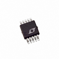
LTC2635CMSE-LMX12#PBF Linear Technology, LTC2635CMSE-LMX12#PBF Datasheet - Page 25

LTC2635CMSE-LMX12#PBF
Manufacturer Part Number
LTC2635CMSE-LMX12#PBF
Description
IC DAC 12BIT I2C QUAD 10MSOP
Manufacturer
Linear Technology
Datasheet
1.LTC2635CMSE-HMI8PBF.pdf
(32 pages)
Specifications of LTC2635CMSE-LMX12#PBF
Settling Time
4.4µs
Number Of Bits
12
Data Interface
I²C
Number Of Converters
4
Voltage Supply Source
Single Supply
Operating Temperature
0°C ~ 70°C
Mounting Type
Surface Mount
Package / Case
10-MSOP Exposed Pad, 10-HMSOP, 10-eMSOP
Lead Free Status / RoHS Status
Lead free / RoHS Compliant
Power Dissipation (max)
-
Available stocks
Company
Part Number
Manufacturer
Quantity
Price
operation
Any channel or combination of channels can be put into
power-down mode by using command 0100b in combi-
nation with the appropriate DAC address, (n). The supply
current is reduced approximately 20% for each DAC
powered down. The integrated reference is automatically
powered down when external reference is selected using
command 0111b. In addition, all the DAC channels and the
integrated reference together can be put into power-down
mode using Power Down Chip command 0101b. When the
integrated reference is in power-down mode, the REF pin
becomes high impedance (typically > 1GΩ). For all power-
down commands the 16-bit data word is ignored.
Normal operation resumes after executing any command
that includes a DAC update, (as shown in Table 1) or pull-
ing the asynchronous LDAC pin low (QFN package only).
The selected DAC is powered up as its voltage output is
updated. When a DAC which is in a powered-down state
is powered up and updated, normal settling is delayed. If
less than four DACs are in a powered-down state prior to
the update command, the power-up delay time is 10µs.
However, if all four DACs and the integrated reference are
powered down, then the main bias generation circuit block
has been automatically shut down in addition to the DAC
amplifiers and reference buffers. In this case, the power up
delay time is 12µs. The power-up of the integrated refer-
ence depends on the command that powered it down. If
the reference is powered down using the Select External
Reference Command (0111b), then it can only be powered
back up using Select Internal Reference Command (0110b).
However, if the reference was powered down using Power
Down Chip Command (0101b), then in addition to Select
Internal Reference Command (0110b), any command (in
software or using the LDAC pin) that powers up the DACs
will also power up the integrated reference.
Voltage Output
The LTC2635’s integrated rail-to-rail amplifier has guar-
anteed load regulation when sourcing or sinking up to
10mA at 5V, and 5mA at 3V.
Load regulation is a measure of the amplifier’s ability to
maintain the rated voltage accuracy over a wide range of
load current. The measured change in output voltage per
change in forced load current is expressed in LSB/mA.
DC output impedance is equivalent to load regulation, and
may be derived from it by simply calculating a change
in units from LSB/mA to Ω. The amplifier’s DC output
impedance is 0.1Ω when driving a load well away from
the rails.
When drawing a load current from either rail, the output
voltage headroom with respect to that rail is limited by
the 50Ω typical channel resistance of the output devices
(e.g., when sinking 1mA, the minimum output voltage is
50Ω • 1mA, or 50mV). See the graph Headroom at Rails
vs. Output Current in the Typical Performance Charac-
teristics section.
The amplifier is stable driving capacitive loads of up to
500pF.
Rail-to-Rail Output Considerations
In any rail-to-rail voltage output device, the output is lim-
ited to voltages within the supply range.
Since the analog output of the DAC cannot go below ground,
it may limit for the lowest codes as shown in Figure 5b.
Similarly, limiting can occur near full-scale when the REF
pin is tied to V
(FSE) is positive, the output for the highest codes limits
at V
occur if V
Offset and linearity are defined and tested over the region
of the DAC transfer function where no output limiting can
occur.
Board Layout
The PC board should have separate areas for the analog and
digital sections of the circuit. A single, solid ground plane
should be used, with analog and digital signals carefully
routed over separate areas of the plane. This keeps digital
signals away from sensitive analog signals and minimizes
the interaction between digital ground currents and the
analog section of the ground plane. The resistance from
the LTC2635 GND pin to the ground plane should be as
low as possible. Resistance here will add directly to the
effective DC output impedance of the device (typically
0.1Ω). Note that the LTC2635 is no more susceptible to
CC
, as shown in Figure 5c. No full-scale limiting can
REF
CC
is less than V
. If V
REF
= V
CC
CC
and the DAC full-scale error
– FSE.
LTC2635
2635fb


