LTC2610IUFD#PBF Linear Technology, LTC2610IUFD#PBF Datasheet
LTC2610IUFD#PBF
Specifications of LTC2610IUFD#PBF
Available stocks


Related parts for LTC2610IUFD#PBF


LTC2610IUFD#PBF Summary of contents
Page 1
... L, LT, LTC, LTM, Linear Technology and the Linear logo are registered trademarks of Linear Technology Corporation. All other trademarks are the property of their respective owners. ...
Page 2
... JA ORDER INFORMATION LEAD FREE FINISH TAPE AND REEL LTC2600CUFD#PBF LTC2600CUFD#TRPBF LTC2600IUFD#PBF LTC2600IUFD#TRPBF LTC2600CGN#PBF LTC2600CGN#TRPBF LTC2600IGN#PBF LTC2600IGN#TRPBF LTC2610CUFD#PBF LTC2610CUFD#TRPBF LTC2610IUFD#PBF LTC2610IUFD#TRPBF LTC2610CGN#PBF LTC2610CGN#TRPBF LTC2610IGN#PBF LTC2610IGN#TRPBF LTC2620CUFD#PBF LTC2620CUFD#TRPBF LTC2620IUFD#PBF LTC2620IUFD#TRPBF LTC2620CGN#PBF LTC2620CGN#TRPBF LTC2620IGN#PBF LTC2620IGN#TRPBF Consult LTC Marketing for parts specifi ed with wider operating temperature ranges. *The temperature grade is identifi label on the shipping container. ...
Page 3
ELECTRICAL CHARACTERISTICS temperature range, otherwise specifi cations are at T SYMBOL PARAMETER CONDITIONS DC Performance Resolution Monotonicity DNL Differential Nonlinearity INL Integral Nonlinearity Load Regulation ...
Page 4
LTC2600/LTC2610/LTC2620 ELECTRICAL CHARACTERISTICS temperature range, otherwise specifi cations are at T SYMBOL PARAMETER Power Supply V Positive Supply Voltage CC I Supply Current CC Digital I/O V Digital Input High Voltage IH V Digital Input Low Voltage IL V Digital ...
Page 5
TIMING CHARACTERISTICS range, otherwise specifi cations are at T SYMBOL PARAMETER V = 2. SDI Valid to SCK Setup 1 t SDI Valid to SCK Hold 2 t SCK High Time 3 t SCK Low Time ...
Page 6
LTC2600/LTC2610/LTC2620 TYPICAL PERFORMANCE CHARACTERISTICS LTC2600 Integral Nonlinearity (INL 4.096V REF –8 –16 –24 –32 0 16384 32768 49152 65535 CODE 2600 G20 DNL vs Temperature 1 ...
Page 7
TYPICAL PERFORMANCE CHARACTERISTICS LTC2610 Integral Nonlinearity (INL 4.096V 6 REF –2 –4 –6 –8 0 4096 8192 12288 16383 CODE 2600 G28 LTC2620 Integral Nonlinearity (INL) 2 ...
Page 8
LTC2600/LTC2610/LTC2620 TYPICAL PERFORMANCE CHARACTERISTICS LTC2600/LTC2610/LTC2620 Zero-Scale Error vs Temperature 3 2.5 2.0 1.5 1.0 0.5 0 –50 –30 – TEMPERATURE (°C) 2600 G04 Gain Error 0.4 0.3 0.2 0.1 0 –0.1 –0.2 –0.3 ...
Page 9
TYPICAL PERFORMANCE CHARACTERISTICS LTC2600/LTC2610/LTC2620 Supply Current vs Logic Voltage 2 SWEEP SCK, SDI 2.3 AND CS/LD 2 2.1 2.0 1.9 1.8 1.7 1.6 1.5 0 0.5 1 1.5 2 2.5 3 3.5 ...
Page 10
LTC2600/LTC2610/LTC2620 PIN FUNCTIONS (GN/UFD) GND (Pin 1/Pin 20): Analog Ground (Pins 2-5 and 12-15/Pins 1-48 and OUTA OUTH 13-16): DAC Analog Voltage Outputs. The output range is 0 – REF REF (Pin 6/Pin 5): Reference ...
Page 11
BLOCK DIAGRAM (20) GND 1 DAC A ( OUTA DAC B V (2) 3 OUTB (3) V DAC C 4 OUTC (4) DAC OUTD REF (5) 6 (7) CS/LD 7 (8) SCK 8 TIMING DIAGRAM ...
Page 12
LTC2600/LTC2610/LTC2620 OPERATION Power-On Reset The LTC2600/LTC2610/LTC2620 clear the outputs to zero-scale when power is fi rst applied, making system initialization consistent and repeatable. For some applications, downstream circuits are active during DAC power-up, and may be sensitive to nonzero outputs ...
Page 13
OPERATION INPUT WORD (LTC2600) COMMAND ADDRESS INPUT WORD (LTC2610) COMMAND ADDRESS INPUT WORD (LTC2620) COMMAND ADDRESS 32-bit sequence. The ...
Page 14
LTC2600/LTC2610/LTC2620 OPERATION Power-Down Mode For power-constrained applications, power-down mode can be used to reduce the supply current whenever less than eight outputs are needed. When in power-down, the buffer amplifi ers and reference inputs are disabled, and draw essentially zero ...
Page 15
OPERATION The GND pin functions both as the node to which the refer- ence and output voltages are referred and as a return path for power currents in the device. Because of this, careful thought should be given to the ...
Page 16
LTC2600/LTC2610/LTC2620 OPERATION 16 2600fe ...
Page 17
OPERATION OUTPUT VOLTAGE 0V NEGATIVE INPUT CODE OFFSET (b) Figure 3. Effects of Rail-to-Rail Operation On a DAC Transfer Curve. (a) Overall Transfer Function (b) Effect of Negative Offset for Codes Near Zero-Scale (c) Effect of Positive Full-Scale Error for ...
Page 18
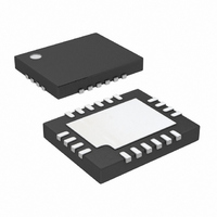
LTC2600/LTC2610/LTC2620 PACKAGE DESCRIPTION 2.65 0.05 4.50 0.05 1.50 REF 3.10 0.05 0.25 0.05 0.50 BSC RECOMMENDED SOLDER PAD PITCH AND DIMENSIONS APPLY SOLDER MASK TO AREAS THAT ARE NOT SOLDERED PIN 1 TOP MARK (NOTE 6) 5.00 0.10 (2 SIDES) ...
Page 19
... Changed “No Connect” pins to “Do Not Connect” in Pin Confi guration and Pin Functions sections Information furnished by Linear Technology Corporation is believed to be accurate and reliable. However, no responsibility is assumed for its use. Linear Technology Corporation makes no representa- tion that the interconnection of its circuits as described herein will not infringe on existing patent rights. ...
Page 20
... GND GND R7 7. LTC2428CG = 4.5V to 5.5V 4.096V CC OUT = 2.7V to 5.5V 2.5V CC OUT = 5V(3V), Low Power, Deglitched OUT = 2.7V to 5.5V, Micropower, Rail-to-Rail Output LT 0510 REV E • PRINTED IN USA © LINEAR TECHNOLOGY CORPORATION 2003 V CC JP1 ON/OFF 3 2 DISABLE ADC 1 R6 7.5k CS SCK 2600fe ...