AD558JN Analog Devices Inc, AD558JN Datasheet
AD558JN
Specifications of AD558JN
Available stocks


Related parts for AD558JN


AD558JN Summary of contents
Page 1
...
Page 2
AD558–SPECIFICATIONS Model Min RESOLUTION 2 RELATIVE ACCURACY +70 C – +125 C OUTPUT 3 Ranges 0 to +2. +10 Current Source +5 Sink Internal Passive Pull-Down to Ground 5 OUTPUT SETTLING TIME 0 ...
Page 3
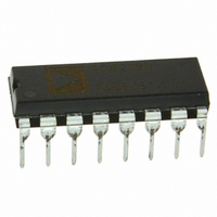
... Exposure to absolute maximum rating conditions for extended periods may affect device reliability. AD558 METALIZATION PHOTOGRAPH Dimensions shown in inches and (mm). Figure 1a. AD558 Pin Configuration (DIP) 1 Model Temperature AD558JN +70 C AD558JP +70 C AD558JD +70 C AD558KN +70 C AD558KP ...
Page 4
AD558 CIRCUIT DESCRIPTION The AD558 consists of four major functional blocks, fabricated on a single monolithic chip (see Figure 2). The main D-to-A converter section uses eight equally-weighted laser-trimmed current sources switched into a silicon-chromium thin-film R/2R resistor ladder network ...
Page 5
OUTPUT AMP 16 500 15 40k 14 14k 2k 13 GND Figure 4. 10.24 V Full-Scale Connection NOTE: Decreasing the scale by putting a resistor in series with GND will not work properly due to the code-dependent currents in GND. ...
Page 6
AD558 DATA t INPUTS DAC V OUTPUT t SETTLING t = STORAGE PULSE WIDTH = 200ns MIN DATA HOLD TIME = 10ns MIN DATA SETUP TIME ...
Page 7
OUTPUT AMP 16 V OUT 15 V SENSE OUT 14 V SELECT OUT 13 AGND Output Range Figure 11. Offset Connection Diagrams INTERFACING THE AD558 TO MICROPROCESSOR DATA BUSES The AD558 is configured to ...
Page 8
AD558 Figure 15. Quiescent Current vs. Power Supply Voltage for AD558 Figure 16. AD558 Settling Characteristics Detail 2.56 V Output Range Full-Scale Step ...