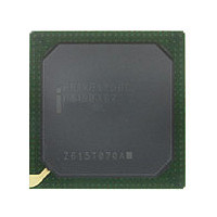
PRIXP425BC 869083 Intel, PRIXP425BC 869083 Datasheet - Page 31

PRIXP425BC 869083
Manufacturer Part Number
PRIXP425BC 869083
Description
Manufacturer
Intel
Datasheet
1.PRIXP425BC_869083.pdf
(130 pages)
Specifications of PRIXP425BC 869083
Core Operating Frequency
400MHz
Package Type
BGA
Pin Count
492
Mounting
Surface Mount
Operating Temperature (max)
70C
Operating Temperature (min)
0C
Operating Temperature Classification
Commercial
Lead Free Status / Rohs Status
Compliant
Intel
2.2.8
2.2.9
2.2.10
August 2006
Document Number: 252479-006US
®
IXP42X product line and IXC1100 control plane processors
The mini-data cache (and D-cache) work with the load buffer and pend buffer to
provide “hit-under-miss” capability that allows the Intel XScale
other data in the cache after a “miss” is encountered. The mini-data cache (and D-
cache) works in conjunction with the write buffer for data that is to be stored to
memory.
Fill Buffer (FB) and Pend Buffer (PB)
The four-entry fill buffer (FB) works with the Intel XScale
cacheable loads until the bus controller can act on them. The FB and the four-entry
pend buffer (PB) work with the D-cache and mini-data cache to provide “hit-under-
miss” capability, allowing the Intel XScale
while “miss” data is being fetched from memory.
The FB can contain up to four unique “miss” addresses (logical), allowing four “misses”
before the processor is stalled. The PB holds up to four addresses (logical) for
additional “misses” to those addresses that are already in the FB. A coprocessor
register can specify draining of the fill and pend (write) buffers.
Write Buffer (WB)
The write buffer (WB) holds data for storage to memory until the bus controller can act
on it. The WB is eight entries deep, where each entry holds 16 bytes. The WB is
constantly enabled and accepts data from the Intel XScale
mini-data cache.
Coprocessor 15, Register 1 specifies whether WB coalescing is enabled or disabled.
When coalescing is disabled, stores to memory occur in program order regardless of
the attribute bits within the descriptors located in the DTLB. When coalescing is
enabled, the attribute bits within the descriptors located in the DTLB are examined to
determine when coalescing is enabled for the destination region of memory. When
coalescing is enabled in both CP15, R1 and the DTLB, data entering the WB can
coalesce with any of the eight entries (16 bytes) and be stored to the destination
memory region, but possibly out of program order.
Stores to a memory region specified to be non-cacheable and non-bufferable by the
attribute bits within the descriptors located in the DTLB causes the processor to stall
until the store completes. A coprocessor register can specify draining of the write
buffer.
Multiply-Accumulate Coprocessor (CP0)
For efficient processing of high-quality, media-and-signal-processing algorithms, CP0
provides 40-bit accumulation of 16 x 16, dual-16 x 16 (SIMD), and 32 x 32 signed
multiplies. Special MAR and MRA instructions are implemented to move the 40-bit
accumulator to two Intel XScale
Intel XScale
accumulator can be stored or loaded to or from D-cache, mini-data cache, or memory
using two STC or LDC instructions.
The 16 x 16 signed multiply-accumulates (MIAxy) multiply either the high/high, low/
low, high/low, or low/high 16 bits of a 32-bit Intel XScale
(multiplier) and another 32-bit Intel XScale
to produce a full, 32-bit product that is sign-extended to 40 bits and added to the 40-
bit accumulator.
®
processor general registers to the 40-bit accumulator (MRA). The 40-bit
Intel
®
IXP42X Product Line of Network Processors and IXC1100 Control Plane Processor
®
processor general registers (MAR) and move two
®
®
processor to seek other data in the caches
processor general register (multiplicand)
®
®
®
processor to hold non-
processor general register
processor, D-cache, or
®
processor to access
Datasheet
31


