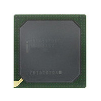
PRIXP425BC 869083 Intel, PRIXP425BC 869083 Datasheet - Page 32
PRIXP425BC 869083
Manufacturer Part Number
PRIXP425BC 869083
Description
Manufacturer
Intel
Datasheet
1.PRIXP425BC_869083.pdf
(130 pages)
Specifications of PRIXP425BC 869083
Core Operating Frequency
400MHz
Package Type
BGA
Pin Count
492
Mounting
Surface Mount
Operating Temperature (max)
70C
Operating Temperature (min)
0C
Operating Temperature Classification
Commercial
Lead Free Status / Rohs Status
Compliant


2.2.11
2.2.12
3.0
Warning:
Intel
Datasheet
32
®
IXP42X Product Line of Network Processors and IXC1100 Control Plane Processor
produce two 16-bits products that are both sign-extended to 40 bits and added to the
40-bit accumulator.
The 32 x 32 signed multiply-accumulates (MIA) multiply a 32-bit, Intel XScale
code can then restart program execution.
The debug unit has two hardware-instruction, break point registers; two hardware,
data-breakpoint registers; and a hardware, data-breakpoint control register. The
second data-breakpoint register can be alternatively used as a mask register for the
first data-breakpoint register.
A 256-entry trace buffer provides the ability to capture control flow messages or
addresses. A JTAG instruction (LDIC) can be used to download a debug handler via the
JTAG port to the mini-instruction cache (the I-cache has a 2-Kbyte, mini-instruction
cache to hold a debug handler).
the particular enabled interface is not being used in the application. These external
resistor requirements are only needed if the particular model of Intel
tolerant.
Dual-signed, 16 x 16 (SIMD) multiply-accumulates (MIAPH) multiply the high/high and
low/low 16-bits of a packed 32-bit, Intel XScale
and another packed 32-bit, Intel XScale
processor general register (multiplier) and another 32-bit, Intel XScale
general register (multiplicand) to produce a 64-bit product where the 40 LSBs are
added to the 40-bit accumulator. The 16 x 32 versions of the 32 x 32 multiply-
accumulate instructions complete in a single cycle.
Performance Monitoring Unit (PMU)
The performance monitoring unit contains two 32-bit, event counters and one 32-bit,
clock counter. The event counters can be programmed to monitor I-cache hit rate, data
caches hit rate, ITLB hit rate, DTLB hit rate, pipeline stalls, BTB prediction hit rate, and
instruction execution count.
Debug Unit
The debug unit is accessed through the JTAG port. The industry-standard, IEEE 1149.1
JTAG port consists of a test access port (TAP) controller, boundary-scan register,
instruction and data registers, and dedicated signals TDI, TDO, TCK, TMS, and TRST#.
The debug unit — when used with debugger application code running on a host system
outside of the Intel XScale
XScale
exception to stop program execution and redirect execution to a debug-handling
routine.
Debug exceptions are instruction breakpoint, data breakpoint, software breakpoint,
external debug breakpoint, exception vector trap, and trace buffer full breakpoint. Once
execution has stopped, the debugger application code can examine or modify the Intel
XScale
Functional Signal Descriptions
Listed in the signal definition tables — starting at
page 34
line and IXC1100 control plane processors has the particular interface enabled and the
interface is not required in the application.
All IXP42X product line and IXC1100 control plane processors I/O pins are not 5-V
®
®
processor, to be debugged. It allows the debugger application code or a debug
processor’s state, coprocessor state, or memory. The debugger application
— are pull-up an pull-down resistor recommendations that are required when
®
processor — allows a program, running on the Intel
Intel
®
IXP42X product line and IXC1100 control plane processors
®
processor general register (multiplicand) to
®
processor general register (multiplier)
Table 7, “SDRAM Interface” on
Document Number: 252479-006US
®
®
IXP42X product
processor
August 2006
®
Related parts for PRIXP425BC 869083
Image
Part Number
Description
Manufacturer
Datasheet
Request
R

Part Number:
Description:
IC NETWRK PROCESSR 400MHZ 492BGA
Manufacturer:
Intel
Datasheet:

Part Number:
Description:
Microprocessor: Intel Celeron M Processor 320 and Ultra Low Voltage Intel Celeron M Processor at 600MHz
Manufacturer:
Intel Corporation
Part Number:
Description:
Intel 82550 Fast Ethernet Multifunction PCI/CardBus Controller
Manufacturer:
Intel Corporation
Datasheet:
Part Number:
Description:
Intel StrataFlash memory 32 Mbit. Access speed 120 ns
Manufacturer:
Intel Corporation
Datasheet:
Part Number:
Description:
Intel StrataFlash memory 32 Mbit. Access speed 120 ns
Manufacturer:
Intel Corporation
Datasheet:
Part Number:
Description:
Intel StrataFlash memory 64 Mbit. Access speed 150 ns
Manufacturer:
Intel Corporation
Datasheet:
Part Number:
Description:
Intel StrataFlash memory 32 Mbit. Access speed 100 ns
Manufacturer:
Intel Corporation
Datasheet:
Part Number:
Description:
DA28F640J5A-1505 Volt Intel StrataFlash Memory
Manufacturer:
Intel Corporation
Datasheet:
Part Number:
Description:
5 Volt Intel StrataFlash?? Memory
Manufacturer:
Intel Corporation
Datasheet:
Part Number:
Description:
5 Volt Intel StrataFlash?? Memory
Manufacturer:
Intel Corporation
Part Number:
Description:
Intel 6300ESB I/O Controller Hub
Manufacturer:
Intel Corporation
Datasheet:
Part Number:
Description:
Intel 82801DB I/O Controller Hub (ICH4), Pb-Free SLI
Manufacturer:
Intel Corporation
Datasheet:
Part Number:
Description:
Intel 82801FB I/O Controller Hub (ICH6)
Manufacturer:
Intel Corporation
Datasheet:
Part Number:
Description:
Intel Strataflash Memory28F128J3 28F640J3 28F320J3
Manufacturer:
Intel Corporation
Datasheet: