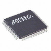
EP1K10TC100-3 Altera, EP1K10TC100-3 Datasheet - Page 31

EP1K10TC100-3
Manufacturer Part Number
EP1K10TC100-3
Description
IC ACEX 1K FPGA 10K 100-TQFP
Manufacturer
Altera
Series
ACEX-1K®r
Datasheet
1.EP1K10TC100-3N.pdf
(86 pages)
Specifications of EP1K10TC100-3
Number Of Logic Elements/cells
576
Number Of Labs/clbs
72
Total Ram Bits
12288
Number Of I /o
66
Number Of Gates
56000
Voltage - Supply
2.375 V ~ 2.625 V
Mounting Type
Surface Mount
Operating Temperature
0°C ~ 70°C
Package / Case
100-TQFP, 100-VQFP
Lead Free Status / RoHS Status
Contains lead / RoHS non-compliant
Other names
544-1027
Available stocks
Company
Part Number
Manufacturer
Quantity
Price
Part Number:
EP1K10TC100-3
Manufacturer:
ALTERA/阿尔特拉
Quantity:
20 000
Part Number:
EP1K10TC100-3N
Manufacturer:
ALTERA/阿尔特拉
Quantity:
20 000
Altera Corporation
On all ACEX 1K devices, the input path from the I/O pad to the FastTrack
Interconnect has a programmable delay element that can be used to
guarantee a zero hold time. Depending on the placement of the IOE
relative to what it is driving, the designer may choose to turn on the
programmable delay to ensure a zero hold time or turn it off to minimize
setup time. This feature is used to reduce setup time for complex pin-to-
register paths (e.g., PCI designs).
Each IOE selects the clock, clear, clock enable, and output enable controls
from a network of I/O control signals called the peripheral control bus.
The peripheral control bus uses high-speed drivers to minimize signal
skew across devices and provides up to 12 peripheral control signals that
can be allocated as follows:
If more than six clock-enable or eight output-enable signals are required,
each IOE on the device can be controlled by clock enable and output
enable signals driven by specific LEs. In addition to the two clock signals
available on the peripheral control bus, each IOE can use one of two
dedicated clock pins. Each peripheral control signal can be driven by any
of the dedicated input pins or the first LE of each LAB in a particular row.
In addition, a LE in a different row can drive a column interconnect, which
causes a row interconnect to drive the peripheral control signal. The chip-
wide reset signal resets all IOE registers, overriding any other control
signals.
When a dedicated clock pin drives IOE registers, it can be inverted for all
IOEs in the device. All IOEs must use the same sense of the clock. For
example, if any IOE uses the inverted clock, all IOEs must use the inverted
clock, and no IOE can use the non-inverted clock. However, LEs can still
use the true or complement of the clock on an LAB-by-LAB basis.
The incoming signal may be inverted at the dedicated clock pin and will
drive all IOEs. For the true and complement of a clock to be used to drive
IOEs, drive it into both global clock pins. One global clock pin will supply
the true, and the other will supply the complement.
When the true and complement of a dedicated input drives IOE clocks,
two signals on the peripheral control bus are consumed, one for each
sense of the clock.
Up to eight output enable signals
Up to six clock enable signals
Up to two clock signals
Up to two clear signals
ACEX 1K Programmable Logic Device Family Data Sheet
31
13


