EP1K10QC208-3 Altera, EP1K10QC208-3 Datasheet - Page 10
EP1K10QC208-3
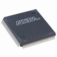
Manufacturer Part Number
EP1K10QC208-3
Description
IC ACEX 1K FPGA 10K 208-PQFP
Manufacturer
Altera
Series
ACEX-1K®r
Datasheet
1.EP1K10TC100-3N.pdf
(86 pages)
Specifications of EP1K10QC208-3
Number Of Logic Elements/cells
576
Number Of Labs/clbs
72
Total Ram Bits
12288
Number Of I /o
120
Number Of Gates
56000
Voltage - Supply
2.375 V ~ 2.625 V
Mounting Type
Surface Mount
Operating Temperature
0°C ~ 70°C
Package / Case
208-MQFP, 208-PQFP
No. Of I/o's
120
Operating Temperature Range
0°C To +70°C
Logic Case Style
QFP
No. Of Pins
208
Peak Reflow Compatible (260 C)
No
No. Of Macrocells
576
Rohs Compliant
No
Clock Management
PLL
Leaded Process Compatible
No
No. Of Gates
10000
No. Of Logic Blocks
72
Lead Free Status / RoHS Status
Contains lead / RoHS non-compliant
Other names
544-1090
Available stocks
Company
Part Number
Manufacturer
Quantity
Price
Company:

Part Number:
EP1K10QC208-3
Manufacturer:
ALTERA
Quantity:
509
Company:
Part Number:
EP1K10QC208-3
Manufacturer:
ALTERA
Quantity:
996
Part Number:
EP1K10QC208-3
Manufacturer:
ALTERA/阿尔特拉
Quantity:
20 000
Company:
Part Number:
EP1K10QC208-3N
Manufacturer:
ALTERA20
Quantity:
288


ACEX 1K Programmable Logic Device Family Data Sheet
Figure 2. ACEX 1K Device in Dual-Port RAM Mode
Notes:
(1)
(2)
10
EAB Local
Interconnect (2)
All registers can be asynchronously cleared by EAB local interconnect signals, global signals, or the chip-wide reset.
EP1K10, EP1K30, and EP1K50 devices have 88 EAB local interconnect channels; EP1K100 devices have 104 EAB
local interconnect channels.
wraddress[ ]
rdaddress[ ]
outclocken
inclocken
outclock
inclock
data[ ]
wren
rden
Dedicated Clocks
Dedicated Inputs &
Global Signals
2
4
The EAB can use Altera megafunctions to implement dual-port RAM
applications where both ports can read or write, as shown in
ACEX 1K EAB can also be used in a single-port mode (see
D
ENA
D
ENA
D
ENA
Q
Q
Q
Note (1)
D
ENA
D
ENA
Generator
Row Interconnect
Pulse
Write
Q
Q
Multiplexers allow read
address and read
enable registers to be
clocked by inclock or
outclock signals.
Data In
Read Address
Write Address
Read Enable
Write Enable
RAM/ROM
1,024
2,048
256
Data Out
512
16
8
4
2
D
ENA
Q
4, 8, 16, 32
Column Interconnect
Altera Corporation
4, 8, 16, 32
Figure
Figure
4, 8
4).
3. The
Related parts for EP1K10QC208-3
Image
Part Number
Description
Manufacturer
Datasheet
Request
R

Part Number:
Description:
CYCLONE II STARTER KIT EP2C20N
Manufacturer:
Altera
Datasheet:


Part Number:
Description:
CPLD, EP610 Family, ECMOS Process, 300 Gates, 16 Macro Cells, 16 Reg., 16 User I/Os, 5V Supply, 35 Speed Grade, 24DIP
Manufacturer:
Altera Corporation
Datasheet:
Part Number:
Description:
CPLD, EP610 Family, ECMOS Process, 300 Gates, 16 Macro Cells, 16 Reg., 16 User I/Os, 5V Supply, 15 Speed Grade, 24DIP
Manufacturer:
Altera Corporation
Datasheet:
Part Number:
Description:
Manufacturer:
Altera Corporation
Datasheet:
Part Number:
Description:
CPLD, EP610 Family, ECMOS Process, 300 Gates, 16 Macro Cells, 16 Reg., 16 User I/Os, 5V Supply, 30 Speed Grade, 24DIP
Manufacturer:
Altera Corporation
Datasheet:
Part Number:
Description:
High-performance, low-power erasable programmable logic devices with 8 macrocells, 10ns
Manufacturer:
Altera Corporation
Datasheet:
Part Number:
Description:
High-performance, low-power erasable programmable logic devices with 8 macrocells, 7ns
Manufacturer:
Altera Corporation
Datasheet:
Part Number:
Description:
Classic EPLD
Manufacturer:
Altera Corporation
Datasheet:
Part Number:
Description:
High-performance, low-power erasable programmable logic devices with 8 macrocells, 10ns
Manufacturer:
Altera Corporation
Datasheet:
Part Number:
Description:
Manufacturer:
Altera Corporation
Datasheet:
Part Number:
Description:
Manufacturer:
Altera Corporation
Datasheet:
Part Number:
Description:
Manufacturer:
Altera Corporation
Datasheet:
Part Number:
Description:
CPLD, EP610 Family, ECMOS Process, 300 Gates, 16 Macro Cells, 16 Reg., 16 User I/Os, 5V Supply, 25 Speed Grade, 24DIP
Manufacturer:
Altera Corporation
Datasheet: