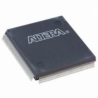
EP1K10QC208-3 Altera, EP1K10QC208-3 Datasheet - Page 13

EP1K10QC208-3
Manufacturer Part Number
EP1K10QC208-3
Description
IC ACEX 1K FPGA 10K 208-PQFP
Manufacturer
Altera
Series
ACEX-1K®r
Datasheet
1.EP1K10TC100-3N.pdf
(86 pages)
Specifications of EP1K10QC208-3
Number Of Logic Elements/cells
576
Number Of Labs/clbs
72
Total Ram Bits
12288
Number Of I /o
120
Number Of Gates
56000
Voltage - Supply
2.375 V ~ 2.625 V
Mounting Type
Surface Mount
Operating Temperature
0°C ~ 70°C
Package / Case
208-MQFP, 208-PQFP
No. Of I/o's
120
Operating Temperature Range
0°C To +70°C
Logic Case Style
QFP
No. Of Pins
208
Peak Reflow Compatible (260 C)
No
No. Of Macrocells
576
Rohs Compliant
No
Clock Management
PLL
Leaded Process Compatible
No
No. Of Gates
10000
No. Of Logic Blocks
72
Lead Free Status / RoHS Status
Contains lead / RoHS non-compliant
Other names
544-1090
Available stocks
Company
Part Number
Manufacturer
Quantity
Price
Company:
Part Number:
EP1K10QC208-3
Manufacturer:
ALTERA
Quantity:
509
Company:
Part Number:
EP1K10QC208-3
Manufacturer:
ALTERA
Quantity:
996
Part Number:
EP1K10QC208-3
Manufacturer:
ALTERA/阿尔特拉
Quantity:
20 000
Company:
Part Number:
EP1K10QC208-3N
Manufacturer:
ALTERA20
Quantity:
288
ACEX 1K Programmable Logic Device Family Data Sheet
If necessary, all EABs in a device can be cascaded to form a single RAM
block. EABs can be cascaded to form RAM blocks of up to 2,048 words
without impacting timing. Altera software automatically combines EABs
to meet a designer’s RAM specifications.
EABs provide flexible options for driving and controlling clock signals.
Different clocks and clock enables can be used for reading and writing to
the EAB. Registers can be independently inserted on the data input, EAB
output, write address, write enable signals, read address, and read enable
signals. The global signals and the EAB local interconnect can drive
write-enable, read-enable, and clock-enable signals. The global signals,
dedicated clock pins, and EAB local interconnect can drive the EAB clock
signals. Because the LEs drive the EAB local interconnect, the LEs can
control write-enable, read-enable, clear, clock, and clock-enable signals.
An EAB is fed by a row interconnect and can drive out to row and column
interconnects. Each EAB output can drive up to two row channels and up
to two column channels; the unused row channel can be driven by other
LEs. This feature increases the routing resources available for EAB
outputs (see
Figures 2
and 4). The column interconnect, which is adjacent
13
to the EAB, has twice as many channels as other columns in the device.
Logic Array Block
An LAB consists of eight LEs, their associated carry and cascade chains,
LAB control signals, and the LAB local interconnect. The LAB provides
the coarse-grained structure to the ACEX 1K architecture, facilitating
efficient routing with optimum device utilization and high performance.
Figure 7
shows the ACEX 1K LAB.
Altera Corporation
13


