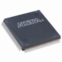
EP1K10QC208-3 Altera, EP1K10QC208-3 Datasheet - Page 37

EP1K10QC208-3
Manufacturer Part Number
EP1K10QC208-3
Description
IC ACEX 1K FPGA 10K 208-PQFP
Manufacturer
Altera
Series
ACEX-1K®r
Datasheet
1.EP1K10TC100-3N.pdf
(86 pages)
Specifications of EP1K10QC208-3
Number Of Logic Elements/cells
576
Number Of Labs/clbs
72
Total Ram Bits
12288
Number Of I /o
120
Number Of Gates
56000
Voltage - Supply
2.375 V ~ 2.625 V
Mounting Type
Surface Mount
Operating Temperature
0°C ~ 70°C
Package / Case
208-MQFP, 208-PQFP
No. Of I/o's
120
Operating Temperature Range
0°C To +70°C
Logic Case Style
QFP
No. Of Pins
208
Peak Reflow Compatible (260 C)
No
No. Of Macrocells
576
Rohs Compliant
No
Clock Management
PLL
Leaded Process Compatible
No
No. Of Gates
10000
No. Of Logic Blocks
72
Lead Free Status / RoHS Status
Contains lead / RoHS non-compliant
Other names
544-1090
Available stocks
Company
Part Number
Manufacturer
Quantity
Price
Company:
Part Number:
EP1K10QC208-3
Manufacturer:
ALTERA
Quantity:
509
Company:
Part Number:
EP1K10QC208-3
Manufacturer:
ALTERA
Quantity:
996
Part Number:
EP1K10QC208-3
Manufacturer:
ALTERA/阿尔特拉
Quantity:
20 000
Company:
Part Number:
EP1K10QC208-3N
Manufacturer:
ALTERA20
Quantity:
288
Altera Corporation
Figure 19. Specifications for the Incoming & Generated Clocks
Note:
(1)
The t
period.
I
ClockLock
Generated
Clock
parameter refers to the nominal input clock period; the t
Input
Clock
t
R
For designs that require both a multiplied and non-multiplied clock, the
clock trace on the board can be connected to the GCLK1 pin. In the Altera
software, the GCLK1 pin can feed both the ClockLock and ClockBoost
circuitry in the ACEX 1K device. However, when both circuits are used,
the other clock pin cannot be used.
ClockLock & ClockBoost Timing Parameters
For the ClockLock and ClockBoost circuitry to function properly, the
incoming clock must meet certain requirements. If these specifications are
not met, the circuitry may not lock onto the incoming clock, which
generates an erroneous clock within the device. The clock generated by
the ClockLock and ClockBoost circuitry must also meet certain
specifications. If the incoming clock meets these requirements during
configuration, the ClockLock and ClockBoost circuitry will lock onto the
clock during configuration. The circuit will be ready for use immediately
after configuration.
specifications.
t
OUTDUTY
t
CLK1
t
F
t
INDUTY
t
t
O
O
ACEX 1K Programmable Logic Device Family Data Sheet
Figure 19
t
I +
t
O +
t
INCLKSTB
t
JITTER
shows the incoming and generated clock
O
parameter refers to the nominal output clock
t
Note (1)
O
t
JITTER
t
I +
t
CLKDEV
37
13


