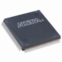
EP1K10QC208-3 Altera, EP1K10QC208-3 Datasheet - Page 40

EP1K10QC208-3
Manufacturer Part Number
EP1K10QC208-3
Description
IC ACEX 1K FPGA 10K 208-PQFP
Manufacturer
Altera
Series
ACEX-1K®r
Datasheet
1.EP1K10TC100-3N.pdf
(86 pages)
Specifications of EP1K10QC208-3
Number Of Logic Elements/cells
576
Number Of Labs/clbs
72
Total Ram Bits
12288
Number Of I /o
120
Number Of Gates
56000
Voltage - Supply
2.375 V ~ 2.625 V
Mounting Type
Surface Mount
Operating Temperature
0°C ~ 70°C
Package / Case
208-MQFP, 208-PQFP
No. Of I/o's
120
Operating Temperature Range
0°C To +70°C
Logic Case Style
QFP
No. Of Pins
208
Peak Reflow Compatible (260 C)
No
No. Of Macrocells
576
Rohs Compliant
No
Clock Management
PLL
Leaded Process Compatible
No
No. Of Gates
10000
No. Of Logic Blocks
72
Lead Free Status / RoHS Status
Contains lead / RoHS non-compliant
Other names
544-1090
Available stocks
Company
Part Number
Manufacturer
Quantity
Price
Company:
Part Number:
EP1K10QC208-3
Manufacturer:
ALTERA
Quantity:
509
Company:
Part Number:
EP1K10QC208-3
Manufacturer:
ALTERA
Quantity:
996
Part Number:
EP1K10QC208-3
Manufacturer:
ALTERA/阿尔特拉
Quantity:
20 000
Company:
Part Number:
EP1K10QC208-3N
Manufacturer:
ALTERA20
Quantity:
288
ACEX 1K Programmable Logic Device Family Data Sheet
40
PCI Pull-Up Clamping Diode Option
ACEX 1K devices have a pull-up clamping diode on every I/O, dedicated
input, and dedicated clock pin. PCI clamping diodes clamp the signal to
the V
diodes can also be used to limit overshoot in other systems.
Clamping diodes are controlled on a pin-by-pin basis. When V
3.3 V, a pin that has the clamping diode option turned on can be driven by
a 2.5-V or 3.3-V signal, but not a 5.0-V signal. When V
that has the clamping diode option turned on can be driven by a 2.5-V
signal, but not a 3.3-V or 5.0-V signal. Additionally, a clamping diode can
be activated for a subset of pins, which allows a device to bridge between
a 3.3-V PCI bus and a 5.0-V device.
Slew-Rate Control
The output buffer in each IOE has an adjustable output slew rate that can
be configured for low-noise or high-speed performance. A slower slew
rate reduces system noise and adds a maximum delay of 4.3 ns. The fast
slew rate should be used for speed-critical outputs in systems that are
adequately protected against noise. Designers can specify the slew rate
pin-by-pin or assign a default slew rate to all pins on a device-wide basis.
The slow slew rate setting affects only the falling edge of the output.
Open-Drain Output Option
ACEX 1K devices provide an optional open-drain output (electrically
equivalent to open-collector output) for each I/O pin. This open-drain
output enables the device to provide system-level control signals (e.g.,
interrupt and write enable signals) that can be asserted by any of several
devices. It can also provide an additional wired-OR plane.
MultiVolt I/O Interface
The ACEX 1K device architecture supports the MultiVolt I/O interface
feature, which allows ACEX 1K devices in all packages to interface with
systems of differing supply voltages. These devices have one set of V
pins for internal operation and input buffers (VCCINT), and another set for
I/O output drivers (VCCIO).
CCIO
value and are required for 3.3-V PCI compliance. Clamping
CCIO
Altera Corporation
is 2.5 V, a pin
CCIO
is
CC


