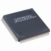
EP2C5Q208C7N Altera, EP2C5Q208C7N Datasheet - Page 63

EP2C5Q208C7N
Manufacturer Part Number
EP2C5Q208C7N
Description
IC CYCLONE II FPGA 5K 208-PQFP
Manufacturer
Altera
Series
Cyclone® IIr
Datasheet
1.EP2C5T144C8N.pdf
(168 pages)
Specifications of EP2C5Q208C7N
Number Of Logic Elements/cells
4608
Number Of Labs/clbs
288
Total Ram Bits
119808
Number Of I /o
142
Voltage - Supply
1.15 V ~ 1.25 V
Mounting Type
Surface Mount
Operating Temperature
0°C ~ 85°C
Package / Case
208-MQFP, 208-PQFP
Family Name
Cyclone® II
Number Of Logic Blocks/elements
4608
# I/os (max)
142
Frequency (max)
402.58MHz
Process Technology
90nm
Operating Supply Voltage (typ)
1.2V
Logic Cells
4608
Ram Bits
119808
Operating Supply Voltage (min)
1.15V
Operating Supply Voltage (max)
1.25V
Operating Temp Range
0C to 85C
Operating Temperature Classification
Commercial
Mounting
Surface Mount
Pin Count
208
Package Type
PQFP
Lead Free Status / RoHS Status
Lead free / RoHS Compliant
Number Of Gates
-
Lead Free Status / Rohs Status
Compliant
Other names
544-1674
Available stocks
Company
Part Number
Manufacturer
Quantity
Price
Company:
Part Number:
EP2C5Q208C7N
Manufacturer:
ALTERA
Quantity:
45
Part Number:
EP2C5Q208C7N
Manufacturer:
ALTERA/阿尔特拉
Quantity:
20 000
Altera Corporation
February 2007
Slew Rate Control
Slew rate control is performed by using programmable output drive
strength.
Bus Hold
Each Cyclone II device user I/O pin provides an optional bus-hold
feature. The bus-hold circuitry can hold the signal on an I/O pin at its
last-driven state. Since the bus-hold feature holds the last-driven state of
the pin until the next input signal is present, an external pull-up or
pull-down resistor is not necessary to hold a signal level when the bus is
tri-stated.
The bus-hold circuitry also pulls undriven pins away from the input
threshold voltage where noise can cause unintended high-frequency
switching. You can select this feature individually for each I/O pin. The
bus-hold output drives no higher than V
signals.
1
The bus-hold circuitry is only active after configuration. When going into
user mode, the bus-hold circuit captures the value on the pin present at
the end of configuration.
The bus-hold circuitry uses a resistor with a nominal resistance (R
approximately 7 kΩ to pull the signal level to the last-driven state. Refer
to the DC Characteristics & Timing Specifications chapter in Volume 1 of the
Cyclone II Device Handbook for the specific sustaining current for each
V
used to identify the next driven input level.
Programmable Pull-Up Resistor
Each Cyclone II device I/O pin provides an optional programmable
pull-up resistor during user mode. If you enable this feature for an I/O
pin, the pull-up resistor (typically 25 kΩ) holds the output to the V
level of the output pin’s bank.
1
CCIO
voltage level driven through the resistor and overdrive current
If the bus-hold feature is enabled, the device cannot use the
programmable pull-up option. Disable the bus-hold feature
when the I/O pin is configured for differential signals. Bus hold
circuitry is not available on the dedicated clock pins.
If the programmable pull-up is enabled, the device cannot use
the bus-hold feature. The programmable pull-up resistors are
not supported on the dedicated configuration, JTAG, and
dedicated clock pins.
Cyclone II Device Handbook, Volume 1
CCIO
to prevent overdriving
Cyclone II Architecture
BH
CCIO
2–51
) of


