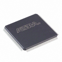
EP1C6T144C8 Altera, EP1C6T144C8 Datasheet - Page 12

EP1C6T144C8
Manufacturer Part Number
EP1C6T144C8
Description
IC CYCLONE FPGA 5980 LE 144-TQFP
Manufacturer
Altera
Series
Cyclone®r
Datasheet
1.EP1C3T144C8.pdf
(106 pages)
Specifications of EP1C6T144C8
Number Of Logic Elements/cells
5980
Number Of Labs/clbs
598
Total Ram Bits
92160
Number Of I /o
98
Voltage - Supply
1.425 V ~ 1.575 V
Mounting Type
Surface Mount
Operating Temperature
0°C ~ 85°C
Package / Case
144-TQFP, 144-VQFP
Family Name
Cyclone®
Number Of Logic Blocks/elements
5980
# I/os (max)
98
Frequency (max)
275.03MHz
Process Technology
0.13um (CMOS)
Operating Supply Voltage (typ)
1.5V
Logic Cells
5980
Ram Bits
92160
Operating Supply Voltage (min)
1.425V
Operating Supply Voltage (max)
1.575V
Operating Temp Range
0C to 85C
Operating Temperature Classification
Commercial
Mounting
Surface Mount
Pin Count
144
Package Type
TQFP
Lead Free Status / RoHS Status
Contains lead / RoHS non-compliant
Number Of Gates
-
Lead Free Status / Rohs Status
Not Compliant
Other names
544-1058
Available stocks
Company
Part Number
Manufacturer
Quantity
Price
Company:
Part Number:
EP1C6T144C8
Manufacturer:
ALTERA
Quantity:
7
Company:
Part Number:
EP1C6T144C8
Manufacturer:
ALTERA
Quantity:
85
Company:
Part Number:
EP1C6T144C8N
Manufacturer:
RAIO
Quantity:
5 600
Company:
Part Number:
EP1C6T144C8N
Manufacturer:
ALTERA
Quantity:
586
Part Number:
EP1C6T144C8N
Manufacturer:
ALTERA/阿尔特拉
Quantity:
20 000
Part Number:
EP1C6T144C8NNY
Manufacturer:
ALTERA
Quantity:
20 000
Cyclone Device Handbook, Volume 1
Figure 2–5. Cyclone LE
2–6
Preliminary
labpre/aload
labclkena1
labclkena2
Chip-Wide
labclk1
labclk2
labclr1
labclr2
Reset
data1
data2
data3
data4
addnsub
Clock Enable
Asynchronous
Clear/Preset/
Load Logic
Clock &
LAB Carry-In
Select
Carry-In1
Carry-In0
Look-Up
Table
(LUT)
Each LE's programmable register can be configured for D, T, JK, or SR
operation. Each register has data, true asynchronous load data, clock,
clock enable, clear, and asynchronous load/preset inputs. Global signals,
general-purpose I/O pins, or any internal logic can drive the register's
clock and clear control signals. Either general-purpose I/O pins or
internal logic can drive the clock enable, preset, asynchronous load, and
asynchronous data. The asynchronous load data input comes from the
data3 input of the LE. For combinatorial functions, the LUT output
bypasses the register and drives directly to the LE outputs.
Each LE has three outputs that drive the local, row, and column routing
resources. The LUT or register output can drive these three outputs
independently. Two LE outputs drive column or row and direct link
routing connections and one drives local interconnect resources. This
allows the LUT to drive one output while the register drives another
output. This feature, called register packing, improves device utilization
because the device can use the register and the LUT for unrelated
Chain
Carry
Register chain
routing from
previous LE
Carry-Out0
Carry-Out1
LAB Carry-Out
Synchronous
LAB-wide
Synchronous
Load
Clear Logic
Load and
Synchronous
LAB-wide
Clear
Register Bypass
Packed
Register Select
ADATA
D
ENA
PRN/ALD
CLRN
Register
Feedback
Q
Programmable
Register
Altera Corporation
LUT chain
routing to next LE
Row, column,
and direct link
routing
Row, column,
and direct link
routing
Local Routing
Register chain
output
May 2008


