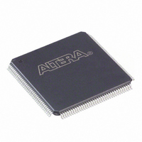
EP1C6T144C8 Altera, EP1C6T144C8 Datasheet - Page 45

EP1C6T144C8
Manufacturer Part Number
EP1C6T144C8
Description
IC CYCLONE FPGA 5980 LE 144-TQFP
Manufacturer
Altera
Series
Cyclone®r
Datasheet
1.EP1C3T144C8.pdf
(106 pages)
Specifications of EP1C6T144C8
Number Of Logic Elements/cells
5980
Number Of Labs/clbs
598
Total Ram Bits
92160
Number Of I /o
98
Voltage - Supply
1.425 V ~ 1.575 V
Mounting Type
Surface Mount
Operating Temperature
0°C ~ 85°C
Package / Case
144-TQFP, 144-VQFP
Family Name
Cyclone®
Number Of Logic Blocks/elements
5980
# I/os (max)
98
Frequency (max)
275.03MHz
Process Technology
0.13um (CMOS)
Operating Supply Voltage (typ)
1.5V
Logic Cells
5980
Ram Bits
92160
Operating Supply Voltage (min)
1.425V
Operating Supply Voltage (max)
1.575V
Operating Temp Range
0C to 85C
Operating Temperature Classification
Commercial
Mounting
Surface Mount
Pin Count
144
Package Type
TQFP
Lead Free Status / RoHS Status
Contains lead / RoHS non-compliant
Number Of Gates
-
Lead Free Status / Rohs Status
Not Compliant
Other names
544-1058
Available stocks
Company
Part Number
Manufacturer
Quantity
Price
Company:
Part Number:
EP1C6T144C8
Manufacturer:
ALTERA
Quantity:
7
Company:
Part Number:
EP1C6T144C8
Manufacturer:
ALTERA
Quantity:
85
Company:
Part Number:
EP1C6T144C8N
Manufacturer:
RAIO
Quantity:
5 600
Company:
Part Number:
EP1C6T144C8N
Manufacturer:
ALTERA
Quantity:
586
Part Number:
EP1C6T144C8N
Manufacturer:
ALTERA/阿尔特拉
Quantity:
20 000
Part Number:
EP1C6T144C8NNY
Manufacturer:
ALTERA
Quantity:
20 000
I/O Structure
Altera Corporation
May 2008
IOEs support many features, including:
■
■
■
■
■
■
■
■
■
■
■
■
Cyclone device IOEs contain a bidirectional I/O buffer and three registers
for complete embedded bidirectional single data rate transfer.
Figure 2–27
register, one output register, and one output enable register. You can use
the input registers for fast setup times and output registers for fast
clock-to-output times. Additionally, you can use the output enable (OE)
register for fast clock-to-output enable timing. The Quartus II software
automatically duplicates a single OE register that controls multiple
output or bidirectional pins. IOEs can be used as input, output, or
bidirectional pins.
Differential and single-ended I/O standards
3.3-V, 64- and 32-bit, 66- and 33-MHz PCI compliance
Joint Test Action Group (JTAG) boundary-scan test (BST) support
Output drive strength control
Weak pull-up resistors during configuration
Slew-rate control
Tri-state buffers
Bus-hold circuitry
Programmable pull-up resistors in user mode
Programmable input and output delays
Open-drain outputs
DQ and DQS I/O pins
shows the Cyclone IOE structure. The IOE contains one input
I/O Structure
Preliminary
2–39


