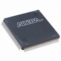
EP1K30QC208-3N Altera, EP1K30QC208-3N Datasheet - Page 2

EP1K30QC208-3N
Manufacturer Part Number
EP1K30QC208-3N
Description
IC ACEX 1K FPGA 30K 208-PQFP
Manufacturer
Altera
Series
ACEX-1K®r
Datasheet
1.EP1K10TC100-3N.pdf
(86 pages)
Specifications of EP1K30QC208-3N
Number Of Logic Elements/cells
1728
Number Of Labs/clbs
216
Total Ram Bits
24576
Number Of I /o
147
Number Of Gates
119000
Voltage - Supply
2.375 V ~ 2.625 V
Mounting Type
Surface Mount
Operating Temperature
0°C ~ 85°C
Package / Case
208-MQFP, 208-PQFP
Family Name
ACEX™ 1K
Number Of Usable Gates
30000
Number Of Logic Blocks/elements
1728
# I/os (max)
147
Frequency (max)
200MHz
Process Technology
CMOS
Operating Supply Voltage (typ)
2.5V
Logic Cells
1728
Ram Bits
24576
Device System Gates
119000
Operating Supply Voltage (min)
2.375V
Operating Supply Voltage (max)
2.625V
Operating Temp Range
0C to 70C
Operating Temperature Classification
Commercial
Mounting
Surface Mount
Pin Count
208
Package Type
PQFP
Lead Free Status / RoHS Status
Lead free / RoHS Compliant
Other names
544-1836
EP1K30QC208-3N
EP1K30QC208-3N
Available stocks
Company
Part Number
Manufacturer
Quantity
Price
Company:
Part Number:
EP1K30QC208-3N
Manufacturer:
ALTERA42
Quantity:
4 571
Part Number:
EP1K30QC208-3N
Manufacturer:
ALTERA/阿尔特拉
Quantity:
20 000
ACEX 1K Programmable Logic Device Family Data Sheet
...and More
Features
2
–
–
–
–
–
–
–
–
Flexible interconnect
–
–
–
–
–
Powerful I/O pins
–
–
–
–
–
-1 speed grade devices are compliant with PCI Local Bus
Specification, Revision 2.2 for 5.0-V operation
Built-in Joint Test Action Group (JTAG) boundary-scan test
(BST) circuitry compliant with IEEE Std. 1149.1-1990, available
without consuming additional device logic.
Operate with a 2.5-V internal supply voltage
In-circuit reconfigurability (ICR) via external configuration
devices, intelligent controller, or JTAG port
ClockLock
clock skew, and clock multiplication
Built-in, low-skew clock distribution trees
100% functional testing of all devices; test vectors or scan chains
are not required
Pull-up on I/O pins before and during configuration
FastTrack
predictable interconnect delays
Dedicated carry chain that implements arithmetic functions such
as fast adders, counters, and comparators (automatically used by
software tools and megafunctions)
Dedicated cascade chain that implements high-speed,
high-fan-in logic functions (automatically used by software tools
and megafunctions)
Tri-state emulation that implements internal tri-state buses
Up to six global clock signals and four global clear signals
Individual tri-state output enable control for each pin
Open-drain option on each I/O pin
Programmable output slew-rate control to reduce switching
noise
Clamp to V
Supports hot-socketing
®
TM
Interconnect continuous routing structure for fast,
CCIO
and ClockBoost
user-selectable on a pin-by-pin basis
TM
options for reduced clock delay,
Altera Corporation


