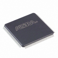
EP1C3T144C6 Altera, EP1C3T144C6 Datasheet - Page 25

EP1C3T144C6
Manufacturer Part Number
EP1C3T144C6
Description
IC CYCLONE FPGA 2910 LE 144-TQFP
Manufacturer
Altera
Series
Cyclone®r
Datasheet
1.EP1C3T144C8.pdf
(106 pages)
Specifications of EP1C3T144C6
Number Of Logic Elements/cells
2910
Number Of Labs/clbs
291
Total Ram Bits
59904
Number Of I /o
104
Voltage - Supply
1.425 V ~ 1.575 V
Mounting Type
Surface Mount
Operating Temperature
0°C ~ 85°C
Package / Case
144-TQFP, 144-VQFP
Lead Free Status / RoHS Status
Contains lead / RoHS non-compliant
Number Of Gates
-
Other names
544-1050
Available stocks
Company
Part Number
Manufacturer
Quantity
Price
Company:
Part Number:
EP1C3T144C6
Manufacturer:
ALTERA
Quantity:
70
Company:
Part Number:
EP1C3T144C6
Manufacturer:
ALTERA
Quantity:
250
Part Number:
EP1C3T144C6
Manufacturer:
ALTERA/阿尔特拉
Quantity:
20 000
Company:
Part Number:
EP1C3T144C6N
Manufacturer:
ALTERA
Quantity:
250
Part Number:
EP1C3T144C6N
Manufacturer:
ALTERA
Quantity:
20 000
Altera Corporation
May 2008
In addition to true dual-port memory, the M4K memory blocks support
simple dual-port and single-port RAM. Simple dual-port memory
supports a simultaneous read and write. Single-port memory supports
non-simultaneous reads and writes.
M4K RAM memory port configurations.
Figure 2–13. Simple Dual-Port and Single-Port Memory Configurations
Note to
(1)
The memory blocks also enable mixed-width data ports for reading and
writing to the RAM ports in dual-port RAM configuration. For example,
the memory block can be written in ×1 mode at port A and read out in ×16
mode from port B.
The Cyclone memory architecture can implement fully synchronous
RAM by registering both the input and output signals to the M4K RAM
block. All M4K memory block inputs are registered, providing
synchronous write cycles. In synchronous operation, the memory block
generates its own self-timed strobe write enable (wren) signal derived
from a global clock. In contrast, a circuit using asynchronous RAM must
generate the RAM wren signal while ensuring its data and address
signals meet setup and hold time specifications relative to the wren
Two single-port memory blocks can be implemented in a single M4K block as long
as each of the two independent block sizes is equal to or less than half of the M4K
block size.
Figure
Simple Dual-Port Memory
Single-Port Memory (1)
2–13:
data[ ]
wraddress[ ]
wren
inclocken
inaclr
data[ ]
address[ ]
wren
inclocken
inaclr
inclock
inclock
Figure 2–13
rdaddress[ ]
outclocken
outclocken
outclock
outclock
outaclr
outaclr
shows these different
rden
q[ ]
q[ ]
Embedded Memory
Preliminary
2–19


