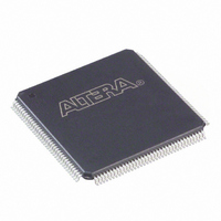
EP1C3T144C6 Altera, EP1C3T144C6 Datasheet - Page 81

EP1C3T144C6
Manufacturer Part Number
EP1C3T144C6
Description
IC CYCLONE FPGA 2910 LE 144-TQFP
Manufacturer
Altera
Series
Cyclone®r
Datasheet
1.EP1C3T144C8.pdf
(106 pages)
Specifications of EP1C3T144C6
Number Of Logic Elements/cells
2910
Number Of Labs/clbs
291
Total Ram Bits
59904
Number Of I /o
104
Voltage - Supply
1.425 V ~ 1.575 V
Mounting Type
Surface Mount
Operating Temperature
0°C ~ 85°C
Package / Case
144-TQFP, 144-VQFP
Lead Free Status / RoHS Status
Contains lead / RoHS non-compliant
Number Of Gates
-
Other names
544-1050
Available stocks
Company
Part Number
Manufacturer
Quantity
Price
Company:
Part Number:
EP1C3T144C6
Manufacturer:
ALTERA
Quantity:
70
Company:
Part Number:
EP1C3T144C6
Manufacturer:
ALTERA
Quantity:
250
Part Number:
EP1C3T144C6
Manufacturer:
ALTERA/阿尔特拉
Quantity:
20 000
Company:
Part Number:
EP1C3T144C6N
Manufacturer:
ALTERA
Quantity:
250
Part Number:
EP1C3T144C6N
Manufacturer:
ALTERA
Quantity:
20 000
Altera Corporation
May 2008
Note to
(1)
M4K
memory
block
Table 4–20. Cyclone Device Performance
Resource
Used
The performance numbers for this function are from an EP1C6 device in a 240-pin PQFP package.
Table
RAM 128 × 36 bit Single port
RAM 128 × 36 bit Simple
RAM 256 × 18 bit True dual-
FIFO 128 × 36 bit
Shift register
9 × 4 × 128
4–20:
Design Size and
Function
Internal Timing Parameters
Internal timing parameters are specified on a speed grade basis
independent of device density.
Cyclone device internal timing microparameters for LEs, IOEs, M4K
memory structures, and MultiTrack interconnects.
t
t
t
t
t
t
t
SU
H
CO
LUT
CLR
PRE
CLKHL
Table 4–21. LE Internal Timing Microparameter Descriptions
dual-port
mode
port mode
Shift
register
Mode
Symbol
—
LEs
40
11
—
—
—
LE register setup time before clock
LE register hold time after clock
LE register clock-to-output delay
LE combinatorial LUT delay for data-in to data-out
Minimum clear pulse width
Minimum preset pulse width
Minimum clock high or low time
Resources Used
Memory
4,608
4,608
4,608
4,608
4,536
M4K
Bits
Tables 4–21
Memory
Blocks
M4K
1
1
1
1
1
Parameter
through
-6 Speed
256.00
255.95
255.95
256.02
255.95
Grade
(MHz)
Performance
4–24
-7 Speed
222.67
222.67
222.67
222.67
222.67
Grade
(MHz)
describe the
Timing Model
Preliminary
-8 Speed
197.01
196.97
196.97
197.01
196.97
Grade
(MHz)
4–11


