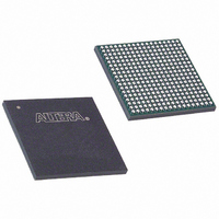
EP1C4F324C8 Altera, EP1C4F324C8 Datasheet - Page 60

EP1C4F324C8
Manufacturer Part Number
EP1C4F324C8
Description
IC CYCLONE FPGA 4K LE 324-FBGA
Manufacturer
Altera
Series
Cyclone®r
Datasheet
1.EP1C3T144C8.pdf
(106 pages)
Specifications of EP1C4F324C8
Number Of Logic Elements/cells
4000
Number Of Labs/clbs
400
Total Ram Bits
78336
Number Of I /o
249
Voltage - Supply
1.425 V ~ 1.575 V
Mounting Type
Surface Mount
Operating Temperature
0°C ~ 85°C
Package / Case
324-FBGA
Lead Free Status / RoHS Status
Contains lead / RoHS non-compliant
Number Of Gates
-
Other names
544-1044
Available stocks
Company
Part Number
Manufacturer
Quantity
Price
Company:
Part Number:
EP1C4F324C8
Manufacturer:
ALTERA
Quantity:
591
Part Number:
EP1C4F324C8
Manufacturer:
ALTERA/阿尔特拉
Quantity:
20 000
Company:
Part Number:
EP1C4F324C8N
Manufacturer:
ALTERA
Quantity:
648
Part Number:
EP1C4F324C8N
Manufacturer:
ALTERA
Quantity:
20 000
Cyclone Device Handbook, Volume 1
2–54
Preliminary
Each I/O bank can support multiple standards with the same V
input and output pins. For example, when V
support LVTTL, LVCMOS, 3.3-V PCI, and SSTL-3 for inputs and outputs.
LVDS I/O Pins
A subset of pins in all four I/O banks supports LVDS interfacing. These
dual-purpose LVDS pins require an external-resistor network at the
transmitter channels in addition to 100-Ω termination resistors on
receiver channels. These pins do not contain dedicated serialization or
deserialization circuitry; therefore, internal logic performs serialization
and deserialization functions.
Table 2–13
device density.
MultiVolt I/O Interface
The Cyclone architecture supports the MultiVolt I/O interface feature,
which allows Cyclone devices in all packages to interface with systems of
different supply voltages. The devices have one set of V
internal operation and input buffers (V
output drivers (V
Note to
(1)
EP1C3
EP1C4
EP1C6
EP1C12
EP1C20
Table 2–13. Cyclone Device LVDS Channels
EP1C3 devices in the 100-pin TQFP package do not support the LVDS I/O
standard.
Device
Table
shows the total number of supported LVDS channels per
2–13:
CCIO
).
Pin Count
100
144
324
400
144
240
256
240
256
324
324
400
CCINT
), and four sets for I/O
Number of LVDS Channels
CCIO
is 3.3-V, a bank can
Altera Corporation
103
129
103
129
(1)
34
29
72
72
66
72
95
CC
pins for
May 2008
CCIO
for


