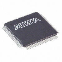
EPF6016ATC100-3 Altera, EPF6016ATC100-3 Datasheet - Page 28

EPF6016ATC100-3
Manufacturer Part Number
EPF6016ATC100-3
Description
IC FLEX 6000 FPGA 16K 100-TQFP
Manufacturer
Altera
Series
FLEX 6000r
Datasheet
1.EPF6010ATC100-3N.pdf
(52 pages)
Specifications of EPF6016ATC100-3
Number Of Logic Elements/cells
1320
Number Of Labs/clbs
132
Number Of I /o
81
Number Of Gates
16000
Voltage - Supply
3 V ~ 3.6 V
Mounting Type
Surface Mount
Operating Temperature
0°C ~ 85°C
Package / Case
100-TQFP, 100-VQFP
Family Name
FLEX 6000
Number Of Usable Gates
16000
Number Of Logic Blocks/elements
1320
# Registers
1320
# I/os (max)
81
Frequency (max)
142.86MHz
Process Technology
SRAM
Operating Supply Voltage (typ)
3.3V
Logic Cells
1320
Device System Gates
16000
Operating Supply Voltage (min)
3V
Operating Supply Voltage (max)
3.6V
Operating Temp Range
0C to 85C
Operating Temperature Classification
Commercial
Mounting
Surface Mount
Pin Count
100
Package Type
TQFP
Lead Free Status / RoHS Status
Contains lead / RoHS non-compliant
Total Ram Bits
-
Lead Free Status / Rohs Status
Not Compliant
Other names
544-1274
Available stocks
Company
Part Number
Manufacturer
Quantity
Price
Part Number:
EPF6016ATC100-3
Manufacturer:
ALTERA/阿尔特拉
Quantity:
20 000
Company:
Part Number:
EPF6016ATC100-3N
Manufacturer:
ALTERA
Quantity:
5 510
Company:
Part Number:
EPF6016ATC100-3N
Manufacturer:
ALTERA
Quantity:
1 200
FLEX 6000 Programmable Logic Device Family Data Sheet
IEEE Std.
1149.1 (JTAG)
Boundary-Scan
Support
28
SAMPLE/PRELOAD Allows a snapshot of the signals at the device pins to be captured and examined during
EXTEST
BYPASS
Table 8. FLEX 6000 JTAG Instructions
JTAG Instruction
normal device operation, and permits an initial data pattern to be output at the device pins.
Allows the external circuitry and board-level interconnections to be tested by forcing a test
pattern at the output pins and capturing test result at the input pins.
Places the 1-bit bypass register between the TDI and TDO pins, which allows the BST
data to pass synchronously through the selected device to adjacent devices during
normal device operation.
Open-drain output pins on 5.0-V or 3.3-V FLEX 6000 devices (with a pull-
up resistor to the 5.0-V supply) can drive 5.0-V CMOS input pins that
require a V
When the pin is inactive, the trace will be pulled up to 5.0 V by the resistor.
The open-drain pin will only drive low or tri-state; it will never drive high.
The rise time is dependent on the value of the pull-up resistor and load
impedance. The I
selecting a pull-up resistor.
Output pins on 5.0-V FLEX 6000 devices with V
a pull-up resistor to the 5.0-V supply) can also drive 5.0-V CMOS input
pins. In this case, the pull-up transistor will turn off when the pin voltage
exceeds 3.3 V. Therefore, the pin does not have to be open-drain.
Power Sequencing & Hot-Socketing
Because FLEX 6000 family devices can be used in a mixed-voltage
environment, they have been designed specifically to tolerate any possible
power-up sequence. The V
in any order.
Signals can be driven into 3.3-V FLEX 6000 devices before and during
power up without damaging the device. Additionally, FLEX 6000 devices
do not drive out during power up. Once operating conditions are reached,
FLEX 6000 devices operate as specified by the user.
All FLEX 6000 devices provide JTAG BST circuitry that comply with the
IEEE Std. 1149.1-1990 specification.
FLEX 6000 devices. JTAG BST can be performed before or after
configuration, but not during configuration (except when you disable
JTAG support in user mode).
1
See
Testing in Altera Devices)
circuitry.
IH
Application Note 39 (IEEE 1149.1 (JTAG) Boundary-Scan
of 3.5 V. When the open-drain pin is active, it will drive low.
OL
current specification should be considered when
CCIO
Description
and V
for more information on JTAG BST
Table 8
CCINT
power planes can be powered
shows JTAG instructions for
CCIO
= 3.3 V or 5.0 V (with
Altera Corporation


