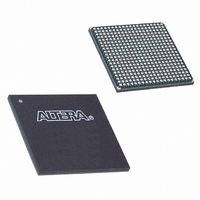
EP1C4F400C8N Altera, EP1C4F400C8N Datasheet - Page 29

EP1C4F400C8N
Manufacturer Part Number
EP1C4F400C8N
Description
IC CYCLONE FPGA 4K LE 400-FBGA
Manufacturer
Altera
Series
Cyclone®r
Datasheet
1.EP1C3T144C8.pdf
(106 pages)
Specifications of EP1C4F400C8N
Number Of Logic Elements/cells
4000
Number Of Labs/clbs
400
Total Ram Bits
78336
Number Of I /o
301
Voltage - Supply
1.425 V ~ 1.575 V
Mounting Type
Surface Mount
Operating Temperature
0°C ~ 85°C
Package / Case
400-FBGA
Lead Free Status / RoHS Status
Lead free / RoHS Compliant
Number Of Gates
-
Other names
544-1806
EP1C4F400C8N
EP1C4F400C8N
Available stocks
Company
Part Number
Manufacturer
Quantity
Price
Company:
Part Number:
EP1C4F400C8N
Manufacturer:
CYCLONE
Quantity:
5 510
Company:
Part Number:
EP1C4F400C8N
Manufacturer:
ALTERA
Quantity:
104
Part Number:
EP1C4F400C8N
Manufacturer:
ALTERA/阿尔特拉
Quantity:
20 000
Company:
Part Number:
EP1C4F400C8NAA
Manufacturer:
ALTERA
Quantity:
3 000
Company:
Part Number:
EP1C4F400C8NAB
Manufacturer:
ALTERA
Quantity:
3 000
Altera Corporation
May 2008
Byte Enables
M4K blocks support byte writes when the write port has a data width of
16, 18, 32, or 36 bits. The byte enables allow the input data to be masked
so the device can write to specific bytes. The unwritten bytes retain the
previous written value.
Control Signals and M4K Interface
The M4K blocks allow for different clocks on their inputs and outputs.
Either of the two clocks feeding the block can clock M4K block registers
(renwe, address, byte enable, datain, and output registers). Only the
output register can be bypassed. The six labclk signals or local
interconnects can drive the control signals for the A and B ports of the
M4K block. LEs can also control the clock_a, clock_b, renwe_a,
renwe_b, clr_a, clr_b, clocken_a, and clocken_b signals, as
shown in
The R4, C4, and direct link interconnects from adjacent LABs drive the
M4K block local interconnect. The M4K blocks can communicate with
LABs on either the left or right side through these row resources or with
LAB columns on either the right or left with the column resources. Up to
10 direct link input connections to the M4K block are possible from the
left adjacent LABs and another 10 possible from the right adjacent LAB.
M4K block outputs can also connect to left and right LABs through 10
direct link interconnects each.
array interface.
Notes to
(1)
(2)
Table 2–5. Byte Enable for M4K Blocks
Any combination of byte enables is possible.
Byte enables can be used in the same manner with 8-bit words, i.e., in ×16 and ×32
modes.
byteena[3..0]
Table
[0] = 1
[1] = 1
[2] = 1
[3] = 1
Figure
2–5:
2–15.
Table 2–5
Figure 2–16
datain ×18
[17..9]
summarizes the byte selection.
[8..0]
—
—
Notes
shows the M4K block to logic
(1),
(2)
Embedded Memory
datain ×36
[26..18]
[35..27]
[17..9]
[8..0]
Preliminary
2–23


