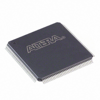
EP2C8T144C7N Altera, EP2C8T144C7N Datasheet - Page 94

EP2C8T144C7N
Manufacturer Part Number
EP2C8T144C7N
Description
IC CYCLONE II FPGA 8K 144-TQFP
Manufacturer
Altera
Series
Cyclone® IIr
Datasheet
1.EP2C5T144C8N.pdf
(168 pages)
Specifications of EP2C8T144C7N
Number Of Logic Elements/cells
8256
Number Of Labs/clbs
516
Total Ram Bits
165888
Number Of I /o
85
Voltage - Supply
1.15 V ~ 1.25 V
Mounting Type
Surface Mount
Operating Temperature
0°C ~ 85°C
Package / Case
144-TQFP, 144-VQFP
Lead Free Status / RoHS Status
Lead free / RoHS Compliant
Number Of Gates
-
Other names
544-1667
Available stocks
Company
Part Number
Manufacturer
Quantity
Price
Company:
Part Number:
EP2C8T144C7N
Manufacturer:
Altera
Quantity:
135
Company:
Part Number:
EP2C8T144C7N
Manufacturer:
ATLERA
Quantity:
10
Operating Conditions
5–4
Cyclone II Device Handbook, Volume 1
Notes to
(1)
(2)
(3)
(4)
(5)
(6)
(7)
R
Table 5–3. DC Characteristics for User I/O, Dual-Purpose, and Dedicated Pins (Part 2 of 2)
CONF
Symbol
All pins, including dedicated inputs, clock, I/O, and JTAG pins, may be driven before V
powered.
The minimum DC input is –0.5 V. During transitions, the inputs may undershoot to –2.0 V or overshoot to the
voltages shown in
dependent upon duty cycle of the signal. The DC case is equivalent to 100% duty cycle.
This value is specified for normal device operation. The value may vary during power-up. This applies for all V
settings (3.3, 2.5, 1.8, and 1.5 V).
Maximum values depend on the actual T
Estimator (www.altera.com) or the Quartus II PowerPlay Power Analyzer feature for maximum values. Refer to
“Power Consumption” on page 5–13
R
not 0 V. Pin pull-up resistance values will be lower if an external source drives the pin higher than V
Minimum condition at –40°C and high V
125°C and low V
These values apply to all V
CONF
(5) (6)
Table
values are based on characterization. R
5–3:
Value of I/O pin
pull-up resistor
before and during
configuration
Recommended
value of I/O pin
external pull-down
resistor before and
during configuration
Parameter
CC
Table
for R
5–4, based on input duty cycle for input currents less than 100 mA. The overshoot is
CONF
Table 5–4
dependency on the duty cycle of the input signal. Refer to
more information.
CCIO
Table 5–4. V
values.
settings.
V
V
V
V
V
IN
IN
IN
IN
IN
for more information.
shows the maximum V
= 0 V; V
= 0 V; V
= 0 V; V
= 0 V; V
= 0 V; V
Maximum V
CC
J
IN
and design utilization. See the Excel-based PowerPlay Early Power
, typical condition at 25°C and nominal V
Overshoot Voltage for All Input Buffers
Conditions
CONF
4.0
4.1
4.2
4.3
4.4
4.5
CCIO
CCIO
CCIO
CCIO
CCIO
(7)
= V
= 3.3 V
= 2.5 V
= 1.8 V
= 1.5 V
= 1.2 V
IN
CCIO
(V)
/I
RCONF
IN
. R
CONF
overshoot voltage and the
Minimum Typical Maximum Unit
values may be different if V
10
15
30
40
50
—
Input Signal Duty Cycle
CC
and maximum condition at
100% (DC)
25
35
50
75
90
1
CCINT
90%
50%
30%
17%
10%
Altera Corporation
and V
Table 5–3
February 2008
100
150
170
50
70
CCIO
2
CCIO
IN
.
are
value is
for
CCIO
kΩ
kΩ
kΩ
kΩ
kΩ
kΩ


