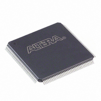
EP1K30TC144-2 Altera, EP1K30TC144-2 Datasheet - Page 12

EP1K30TC144-2
Manufacturer Part Number
EP1K30TC144-2
Description
IC ACEX 1K FPGA 30K 144-TQFP
Manufacturer
Altera
Series
ACEX-1K®r
Datasheet
1.EP1K10TC100-3N.pdf
(86 pages)
Specifications of EP1K30TC144-2
Number Of Logic Elements/cells
1728
Number Of Labs/clbs
216
Total Ram Bits
24576
Number Of I /o
102
Number Of Gates
119000
Voltage - Supply
2.375 V ~ 2.625 V
Mounting Type
Surface Mount
Operating Temperature
0°C ~ 70°C
Package / Case
144-TQFP, 144-VQFP
Family Name
ACEX™ 1K
Number Of Usable Gates
30000
Number Of Logic Blocks/elements
1728
# I/os (max)
102
Frequency (max)
200MHz
Process Technology
CMOS
Operating Supply Voltage (typ)
2.5V
Logic Cells
1728
Ram Bits
24576
Device System Gates
119000
Operating Supply Voltage (min)
2.375V
Operating Supply Voltage (max)
2.625V
Operating Temp Range
0C to 70C
Operating Temperature Classification
Commercial
Mounting
Surface Mount
Pin Count
144
Package Type
TQFP
Lead Free Status / RoHS Status
Contains lead / RoHS non-compliant
Other names
544-1066
Available stocks
Company
Part Number
Manufacturer
Quantity
Price
Company:
Part Number:
EP1K30TC144-2
Manufacturer:
ALTERA
Quantity:
1 831
Company:
Part Number:
EP1K30TC144-2
Manufacturer:
ALTERA
Quantity:
155
Part Number:
EP1K30TC144-2
Manufacturer:
ALTERA/阿尔特拉
Quantity:
20 000
Company:
Part Number:
EP1K30TC144-2N
Manufacturer:
ALTERA
Quantity:
1 500
Company:
Part Number:
EP1K30TC144-2N
Manufacturer:
ALTERA
Quantity:
5 510
ACEX 1K Programmable Logic Device Family Data Sheet
Figure 5. ACEX 1K EAB Memory Configurations
Figure 6. Examples of Combining ACEX 1K EABs
12
256
256
256
16
16
16
EABs can be used to implement synchronous RAM, which is easier to use
than asynchronous RAM. A circuit using asynchronous RAM must
generate the RAM write enable signal, while ensuring that its data and
address signals meet setup and hold time specifications relative to the
write enable signal. In contrast, the EAB’s synchronous RAM generates its
own write enable signal and is self-timed with respect to the input or write
clock. A circuit using the EAB’s self-timed RAM must only meet the setup
and hold time specifications of the global clock.
When used as RAM, each EAB can be configured in any of the following
sizes: 256 16; 512 8; 1,024
EAB memory configurations.
Larger blocks of RAM are created by combining multiple EABs. For
example, two 256 16 RAM blocks can be combined to form a 256 32
block, and two 512 8 RAM blocks can be combined to form a
512 16 block.
256
32
512
Figure 6
8
shows examples of multiple EAB combination.
4; or 2,048 2.
1,024 4
512
512
8
8
Figure 5
512
16
2,048 2
shows the ACEX 1K
Altera Corporation


