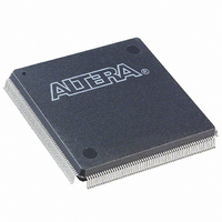
EPF81500AQC240-2 Altera, EPF81500AQC240-2 Datasheet - Page 21

EPF81500AQC240-2
Manufacturer Part Number
EPF81500AQC240-2
Description
IC FLEX 8000A FPGA 16K 240-PQFP
Manufacturer
Altera
Series
FLEX 8000r
Datasheet
1.EPF8282ATC100-3.pdf
(62 pages)
Specifications of EPF81500AQC240-2
Number Of Logic Elements/cells
1296
Number Of Labs/clbs
162
Number Of I /o
181
Number Of Gates
16000
Voltage - Supply
4.75 V ~ 5.25 V
Mounting Type
Surface Mount
Operating Temperature
0°C ~ 85°C
Package / Case
240-MQFP, 240-PQFP
Family Name
FLEX 8000
Number Of Usable Gates
16000
Number Of Logic Blocks/elements
1296
# Registers
1500
# I/os (max)
181
Frequency (max)
125MHz
Process Technology
CMOS
Operating Supply Voltage (typ)
5V
Logic Cells
1296
Ram Bits
8
Device System Gates
16000
Operating Supply Voltage (min)
4.75V
Operating Supply Voltage (max)
5.25V
Operating Temp Range
0C to 70C
Operating Temperature Classification
Commercial
Mounting
Surface Mount
Pin Count
240
Package Type
PQFP
Lead Free Status / RoHS Status
Contains lead / RoHS non-compliant
Total Ram Bits
-
Lead Free Status / Rohs Status
Not Compliant
Other names
544-2249
Available stocks
Company
Part Number
Manufacturer
Quantity
Price
Company:
Part Number:
EPF81500AQC240-2
Manufacturer:
ALTERA
Quantity:
135
Part Number:
EPF81500AQC240-2
Manufacturer:
ALTERA/阿尔特拉
Quantity:
20 000
Altera Corporation
Figure 12. FLEX 8000 Column-to-IOE Connections
In addition to general-purpose I/O pins, FLEX 8000 devices have four
dedicated input pins. These dedicated inputs provide low-skew, device-
wide signal distribution, and are typically used for global clock, clear, and
preset control signals. The signals from the dedicated inputs are available
as control signals for all LABs and I/O elements in the device. The
dedicated inputs can also be used as general-purpose data inputs because
they can feed the local interconnect of each LAB in the device.
Signals enter the FLEX 8000 device either from the I/O pins that provide
general-purpose input capability or from the four dedicated inputs. The
IOEs are located at the ends of the row and column interconnect channels.
I/O pins can be used as input, output, or bidirectional pins. Each I/O pin
has a register that can be used either as an input register for external data
that requires fast setup times, or as an output register for data that
requires fast clock-to-output performance. The MAX+PLUS II Compiler
uses the programmable inversion option to invert signals automatically
from the row and column interconnect when appropriate.
The clock, clear, and output enable controls for the IOEs are provided by
a network of I/O control signals. These signals can be supplied by either
the dedicated input pins or by internal logic. The IOE control-signal paths
are designed to minimize the skew across the device. All control-signal
sources are buffered onto high-speed drivers that drive the signals around
the periphery of the device. This “peripheral bus” can be configured to
provide up to four output enable signals (10 in EPF81500A devices), and
up to two clock or clear signals.
output enable signals are shared with one clock and one clear signal.
Each IOE is
driven by an
8-to-1
multiplexer.
FLEX 8000 Programmable Logic Device Family Data Sheet
IOE
8
Column Interconnect
Figure 13 on page 22
16
IOE
8
shows how two
Each IOE can drive
up to two column
signals.
21
3


