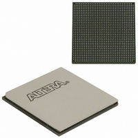
EP3SL150F1152C3N Altera, EP3SL150F1152C3N Datasheet - Page 201

EP3SL150F1152C3N
Manufacturer Part Number
EP3SL150F1152C3N
Description
IC STRATX III FPGA 150K 1152FBGA
Manufacturer
Altera
Series
Stratix® IIIr
Datasheets
1.EP3SL150F780C4N.pdf
(16 pages)
2.EP3SL150F780C4N.pdf
(332 pages)
3.EP3SL150F780C4N.pdf
(456 pages)
Specifications of EP3SL150F1152C3N
Number Of Logic Elements/cells
142500
Number Of Labs/clbs
5700
Total Ram Bits
6390
Number Of I /o
744
Voltage - Supply
0.86 V ~ 1.15 V
Mounting Type
Surface Mount
Operating Temperature
0°C ~ 85°C
Package / Case
1152-FBGA
For Use With
544-2568 - KIT DEVELOPMENT STRATIX III
Lead Free Status / RoHS Status
Lead free / RoHS Compliant
Number Of Gates
-
Other names
544-2408
EP3SL150F1152C3NES
EP3SL150F1152C3NES
Available stocks
Company
Part Number
Manufacturer
Quantity
Price
Company:
Part Number:
EP3SL150F1152C3N
Manufacturer:
ALTERA
Quantity:
490
- Current page: 201 of 456
- Download datasheet (7Mb)
Chapter 6: Clock Networks and PLLs in Stratix III Devices
Chapter Revision History
Chapter Revision History
Table 6–23. Chapter Revision History (Part 1 of 2)
© July 2010
July 2010
March 2010
July 2009
May 2009
February 2009
October 2008
May 2008
November 2007
Date
Altera Corporation
Table 6–23
Version
2.0
1.9
1.8
1.7
1.6
1.5
1.4
1.3
lists the revision history for this chapter.
Updated
Updated for the Quartus II software version 9.1 SP2 release:
■
■
■
■
■
■
■
■
■
■
■
■
■
■
■
■
■
■
■
■
■
■
■
■
■
■
■
Updated “pfdena” on page 6–42.
Updated Table 6–10 and Table 6–11.
Updated Figure 6–42.
Updated the “Guidelines” and “PLL Cascading and Clock Network Guidelines”
sections.
Removed “sub-regional clock networks” information.
Minor text edits.
Updated “Clock Switchover” section.
Updated Figure 6–37.
Added “PLL and Clock Network Guidelines for External Memory Interface” and
“Zero-Delay Buffer Mode” sections.
Updated Figure 6–17.
Updated Table 6–7 and Table 6–10.
Updated Figure 6–23.
Updated “PLL Clock I/O Pins”, “Logic Array Blocks (LABs)”, and “Clock Feedback
Modes” sections.
Removed “Reference Documents” section.
Updated Table 6–10, Table 6–13, and Table 6–14.
Updated “locked”, “Manual Override”, “Bypassing PLL”, “PLL Clock I/O Pins”, and
“Dynamic Phase-Shifting” sections.
Updated Figure 6–22, Figure 6–24, and Figure 6–26.
Updated (Note 2) to Figure 6–22.
Added (Note 3) to Table 6–14.
Added Figure 6–27.
Updated New Document Format.
Updated Table 6–3, Table 6–4, Table 6–5, Table 6–6, Table 6–7, and Table 6–14.
Added new Figure 6–5 through Figure 6–9 to “Periphery Clock Networks” section.
Updated “Logic Array Blocks (LABs)”, “External Feedback Mode”, “Phase-Shift
Implementation”, and “Spread-Spectrum Tracking” sections.
Updated notes to Figure 6–17.
Updated notes to Figure 6–22.
Updated notes to Figure 6–27.
Updated Figure 6–43.
Figure
6–44.
Changes Made
Stratix III Device Handbook, Volume 1
6–53
Related parts for EP3SL150F1152C3N
Image
Part Number
Description
Manufacturer
Datasheet
Request
R

Part Number:
Description:
CYCLONE II STARTER KIT EP2C20N
Manufacturer:
Altera
Datasheet:

Part Number:
Description:
CPLD, EP610 Family, ECMOS Process, 300 Gates, 16 Macro Cells, 16 Reg., 16 User I/Os, 5V Supply, 35 Speed Grade, 24DIP
Manufacturer:
Altera Corporation
Datasheet:

Part Number:
Description:
CPLD, EP610 Family, ECMOS Process, 300 Gates, 16 Macro Cells, 16 Reg., 16 User I/Os, 5V Supply, 15 Speed Grade, 24DIP
Manufacturer:
Altera Corporation
Datasheet:

Part Number:
Description:
Manufacturer:
Altera Corporation
Datasheet:

Part Number:
Description:
CPLD, EP610 Family, ECMOS Process, 300 Gates, 16 Macro Cells, 16 Reg., 16 User I/Os, 5V Supply, 30 Speed Grade, 24DIP
Manufacturer:
Altera Corporation
Datasheet:

Part Number:
Description:
High-performance, low-power erasable programmable logic devices with 8 macrocells, 10ns
Manufacturer:
Altera Corporation
Datasheet:

Part Number:
Description:
High-performance, low-power erasable programmable logic devices with 8 macrocells, 7ns
Manufacturer:
Altera Corporation
Datasheet:

Part Number:
Description:
Classic EPLD
Manufacturer:
Altera Corporation
Datasheet:

Part Number:
Description:
High-performance, low-power erasable programmable logic devices with 8 macrocells, 10ns
Manufacturer:
Altera Corporation
Datasheet:

Part Number:
Description:
Manufacturer:
Altera Corporation
Datasheet:

Part Number:
Description:
Manufacturer:
Altera Corporation
Datasheet:

Part Number:
Description:
Manufacturer:
Altera Corporation
Datasheet:

Part Number:
Description:
CPLD, EP610 Family, ECMOS Process, 300 Gates, 16 Macro Cells, 16 Reg., 16 User I/Os, 5V Supply, 25 Speed Grade, 24DIP
Manufacturer:
Altera Corporation
Datasheet:


